


Physical Vapor Deposition (PVD) is one of the most widely used thin-film coating technologies in modern manufacturing. It is extensively applied in semiconductors, optics, solar energy, decorative coatings, cutting tools, medical devices, and many other high-tech industries.
At the heart of every PVD process is the sputtering target. The quality, purity, and composition of the target directly influence coating performance, deposition efficiency, and production consistency. Selecting the appropriate target material is therefore essential for achieving reliable and high-quality thin films.
What Is a PVD Sputtering Target?
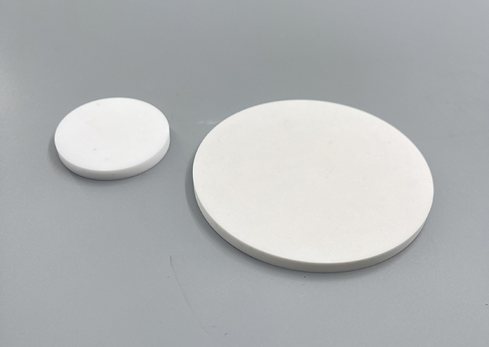
A sputtering target is the source material used during the PVD coating process. Under plasma bombardment, atoms are ejected from the target surface and deposited onto a substrate, forming a thin film with specific physical, chemical, or optical properties.
Depending on the application, sputtering targets are manufactured from pure metals, alloys, ceramics, semiconductors, precious metals, or composite materials. Their purity, density, grain structure, and dimensional accuracy all play an important role in coating quality and target utilization.
How Does PVD Work?
PVD is a vacuum deposition process that converts solid materials into vapor and deposits them onto a substrate as a thin film. Although several PVD techniques exist, such as magnetron sputtering and evaporation, the basic process consists of three stages:
- Material Vaporization – Energy from plasma, electron beams, or other sources releases atoms from the target material.
- Particle Transport – The released atoms travel through a high-vacuum environment toward the substrate.
- Film Deposition – The atoms condense on the substrate surface, forming a dense and uniform coating.
Because the process takes place under vacuum conditions, PVD coatings typically provide high purity, excellent uniformity, and strong adhesion.
PVD vs. CVD
PVD and Chemical Vapor Deposition (CVD) are the two most common thin-film deposition technologies. While both produce functional coatings, their deposition mechanisms differ.
| Feature | PVD | CVD |
|---|---|---|
| Deposition Method | Physical vaporization | Chemical reaction |
| Process Temperature | Lower | Higher |
| Process Environment | High vacuum | Vacuum or atmospheric pressure |
| Film Purity | Very high | High |
| Typical Applications | Semiconductors, optics, decorative and hard coatings | Integrated circuits, protective coatings, complex geometries |
PVD is generally preferred when high-purity coatings, low processing temperatures, and precise thickness control are required.
Types of PVD Sputtering Targets
Sputtering targets can be classified according to their material composition and intended application.
| Target Type | Typical Materials | Common Applications |
|---|---|---|
| Metal Targets | Cu, Al, Ti, Cr, Ni, Mo | Conductive films, semiconductor devices |
| Alloy Targets | ITO, AZO, NiCr, AlSi | Transparent conductive and functional coatings |
| Ceramic Targets | Al₂O₃, SiO₂, TiO₂, ZrO₂ | Optical coatings, insulating layers |
| Semiconductor Targets | Si, Ge | Microelectronics, MEMS, photovoltaics |
| Rare Earth Targets | Y₂O₃, CeO₂, La₂O₃ | Optical and electronic materials |
| Precious Metal Targets | Au, Ag, Pt, Pd | Decorative coatings, sensors, electrical contacts |
| Composite Targets | Doped oxides and customized materials | Advanced functional thin films |
Each target material offers unique electrical, optical, thermal, or mechanical properties, making proper selection critical for different coating applications.
How to Choose the Right Sputtering Target
Selecting the right target begins with understanding the coating requirements.
First, determine the desired film properties, such as electrical conductivity, hardness, corrosion resistance, transparency, or thermal stability. Next, ensure the target material is compatible with both the substrate and the deposition process. Factors such as purity, density, grain structure, deposition rate, target utilization, and production cost should also be considered.
The following table provides general guidance for target selection.
| Coating Requirement | Recommended Target Materials |
|---|---|
| High Electrical Conductivity | Copper (Cu), Aluminum (Al) |
| High Hardness | Titanium (Ti), Chromium (Cr) |
| Optical Transparency | ITO, AZO |
| High Reflectivity | Silver (Ag), Aluminum (Al) |
| Wear Resistance | Titanium-based and Chromium-based targets |
| Corrosion Resistance | Chromium (Cr), Titanium (Ti) |
Choosing the appropriate target helps improve coating quality, production efficiency, and overall manufacturing cost.
Manufacturing and Processing of Sputtering Targets
The performance of a sputtering target depends not only on its chemical composition but also on its manufacturing process.
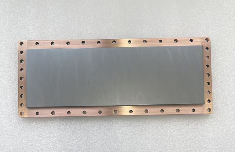
Two of the most common production methods are powder metallurgy and vacuum melting. Powder metallurgy is widely used for refractory metals, ceramics, and composite materials, while vacuum melting is commonly employed for high-purity metals and alloy targets.
After fabrication, targets undergo precision machining, grinding, polishing, cleaning, and quality inspection to ensure accurate dimensions, smooth surfaces, high density, and defect-free internal structures.
Strict quality control helps achieve stable sputtering performance and consistent thin-film deposition.
Applications of PVD Sputtering Targets
PVD sputtering targets are used across a wide range of advanced manufacturing industries.
In the semiconductor industry, they are used to deposit conductive, barrier, and insulating layers for integrated circuits and electronic devices.
In optical coating, oxide and metallic targets are used to produce anti-reflection coatings, mirrors, filters, and precision optical components.
For decorative coatings, precious metals, titanium, and chromium-based targets provide durable and attractive finishes for watches, jewelry, consumer electronics, and architectural hardware.
In cutting tools and industrial molds, titanium- and chromium-based targets are widely used to deposit hard coatings that improve wear resistance, hardness, and corrosion protection.
PVD coatings are also widely applied in automotive, aerospace, medical devices, solar energy, display technology, and other high-performance industrial sectors.
Conclusion
Sputtering targets are the foundation of every successful PVD coating process. Their material composition, purity, density, and manufacturing quality directly influence coating performance, process stability, and production efficiency.
Understanding the characteristics of different target materials and selecting the appropriate solution for each application helps manufacturers achieve reliable, high-quality thin films while optimizing production costs.
VIMATERIAL supplies a comprehensive range of high-purity sputtering targets, including pure metals, alloys, ceramics, rare earth materials, and customized compositions for semiconductor, optical, photovoltaic, research, and industrial coating applications.
Frequently Asked Questions (FAQs)
What is a PVD sputtering target?
A sputtering target is the source material used in the Physical Vapor Deposition (PVD) process. During sputtering, atoms are ejected from the target by plasma and deposited onto a substrate to form a thin film with specific electrical, optical, mechanical, or chemical properties.
What materials are commonly used for PVD sputtering targets?
PVD sputtering targets are available in a wide range of materials, including pure metals, alloys, ceramics, semiconductors, rare earth compounds, and precious metals. Common examples include aluminum (Al), copper (Cu), titanium (Ti), chromium (Cr), silicon (Si), indium tin oxide (ITO), aluminum oxide (Al₂O₃), and titanium dioxide (TiO₂).
How do I choose the right sputtering target?
The ideal sputtering target depends on your coating requirements. Key factors include the desired film properties, substrate compatibility, target purity, deposition rate, operating conditions, and production cost. Selecting the appropriate material helps improve coating quality, process stability, and target utilization.
What is the difference between metal and ceramic sputtering targets?
Metal targets generally provide excellent electrical conductivity and are widely used for conductive films and semiconductor applications. Ceramic targets are typically used for insulating, optical, and protective coatings because of their excellent chemical stability, high hardness, and corrosion resistance.
Why is target purity important?
High-purity sputtering targets help reduce contamination during deposition, resulting in improved film quality, better process repeatability, and enhanced device performance. Semiconductor and optical coating applications often require target purities of 99.99% (4N) or higher.
Which industries use PVD sputtering targets?
PVD sputtering targets are widely used in semiconductor manufacturing, optical coatings, flat-panel displays, solar cells, cutting tools, decorative coatings, medical devices, automotive components, aerospace, and scientific research.
Can sputtering targets be customized?
Yes. Sputtering targets can be manufactured in customized dimensions, shapes, compositions, and bonding configurations to meet specific deposition equipment and application requirements. Customized solutions are commonly used in research laboratories and industrial production.
References
- [1] Ohring, M. Materials Science of Thin Films: Deposition and Structure. 2nd Edition. Academic Press, 2002.
- [2] Mattox, D. M. Handbook of Physical Vapor Deposition (PVD) Processing. 2nd Edition. William Andrew Publishing, 2010.
- [3] Bunshah, R. F. Handbook of Deposition Technologies for Films and Coatings. 3rd Edition. William Andrew Publishing.
- [4] Kelly, P. J.; Arnell, R. D. Magnetron Sputtering: A Review of Recent Developments and Applications. Vacuum, 56(3), 159–172 (2000).
- [5] ASM International. ASM Handbook, Volume 5: Surface Engineering.
- [6] Handbook of Thin Film Deposition. 5th Edition. Elsevier.
Further Reading
Need a Custom Material Solution?
VIMATERIAL supplies high-purity sputtering targets, evaporation materials, advanced ceramic materials, battery materials, and rare earth compounds for semiconductor, optical, energy, and industrial applications.
Our engineering team also provides customized material solutions based on your specifications and application requirements.