| Product ID | Formula | Purity | Dimension | Quantity | Price in € | Inquiry |
|---|---|---|---|---|---|---|
| 221401ST001 | TiSi2 | 99.9% | Ø 50.8mm x 3.175mm | 1 | POR | Inquire |
| 221401ST002 | TiSi2 | 99.9% | Ø 50.8mm x 6.35mm | 1 | POR | Inquire |
| 221401ST003 | TiSi2 | 99.9% | Ø 76.2mm x 3.175mm | 1 | POR | Inquire |
| 221401ST004 | TiSi2 | 99.9% | Ø 76.2mm x 6.35mm | 1 | POR | Inquire |
| 221401ST005 | TiSi2 | 99.9% | Ø 101.6mm x 3.175mm | 1 | POR | Inquire |
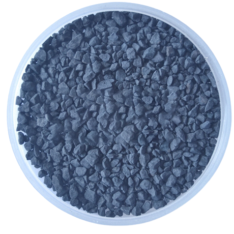
Titanium disilicide sputtering target TiSi2 is a compound target composed of titanium and silicon, mainly used in semiconductor, integrated circuit and other fields, through the sputtering process to deposit TiSi₂ thin film used to reduce the contact resistance, improve the performance of the device and so on many aspects.
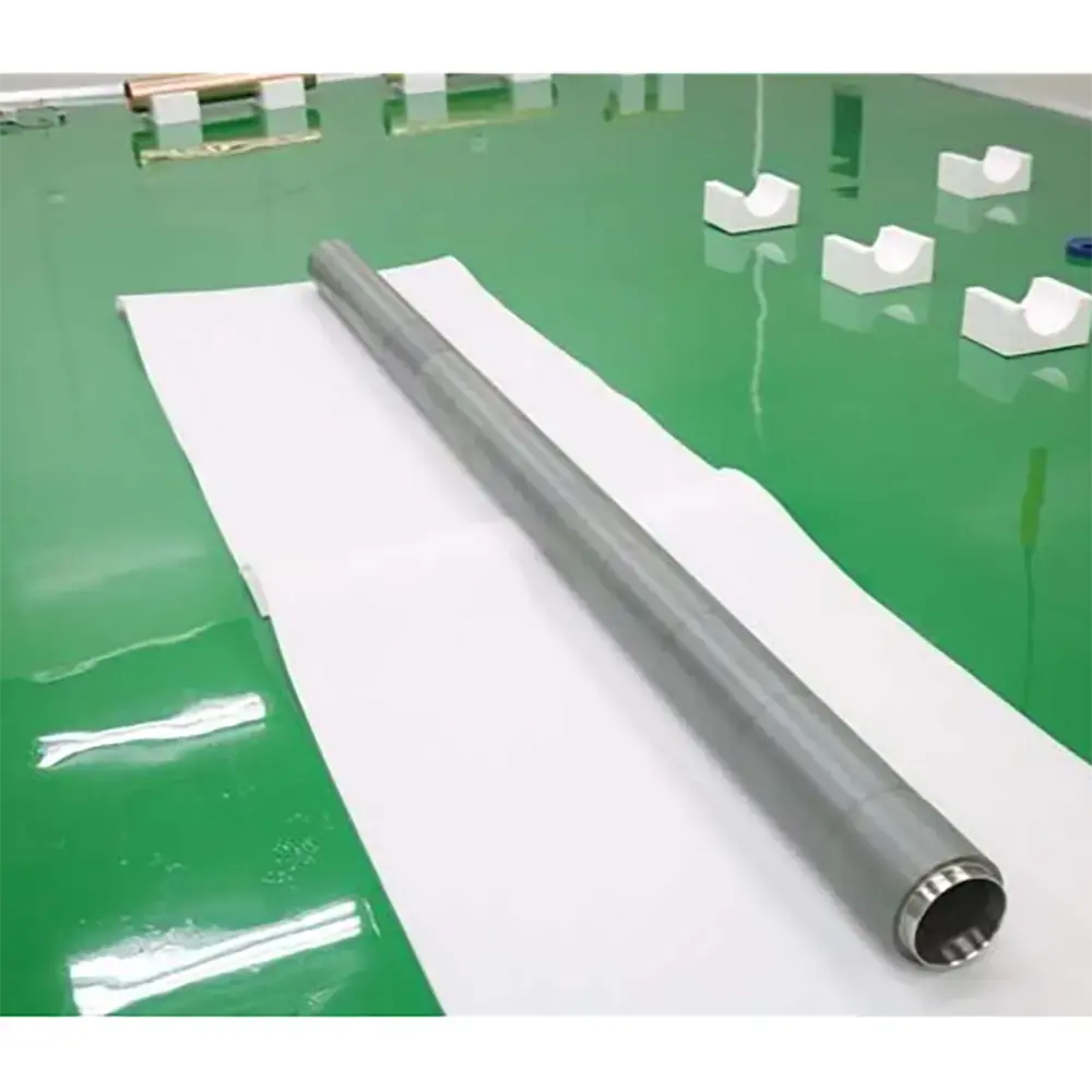
We supply Titanium disilicide sputtering targets, VIMATERIAL can also provide target binding service, our products are subject to customisation and experimentation, please contact us if you need.
Molecular Formula: TiSi₂
Molecular weight: 104.04 g/mol
Appearance: Usually grey or black solid
Density: about 4.39 g/cm³.
Melting point: about 1540°C
Crystal structure: It has two crystal structures, C49 (low temperature phase) and C54 (high temperature phase), the C49 structure is a substable phase, and the C54 structure is a thermodynamically stable phase, and it can be transformed from the C49 phase to the C54 phase under suitable temperature treatment, and the transformation of this crystal structure has an important effect on its electrical and other properties.
Semiconductor field:Titanium silicide sputtering targets are used in semiconductor manufacturing to form a silicide layer during the metallisation process of the chip, which effectively reduces the contact resistance between the source, drain and silicon and improves the chip performance.
Integrated Circuits: In integrated circuits, the TiSi₂ film formed by sputtering the target can be used as part of the interconnecting wires, which improves the conductivity of the circuit and the speed of the signal transmission, and enhances the integration and operational efficiency of the integrated circuits.
Photovoltaic field: Titanium disilicide sputtering target used in the preparation of electrode materials for photovoltaic cells, it can enhance the electrical contact between the electrode and the semiconductor material and improve the photoelectric conversion efficiency of the cell.
Micro Electro Mechanical Systems (MEMS) field: In MEMS device fabrication, TiSi₂ sputtered thin films can be used as structural or conductive materials to help build micro- and nano-sized mechanical and electronic components, which support miniaturisation and high performance of MEMS devices.
Our products are subject to a strict quality management system. There are strict inspection standards for incoming materials, processing, final inspection and factory inspection. Strict isolation measures are taken for unqualified processing to prevent unqualified products from flowing into the next process. Samples are provided for customer re-inspection according to customer requirements.
Titanium disilicide TiSi2 sputtering targets are packed in double-layer vacuum bags and then boxed, and packed in cartons outside.
Titanium disilicide sputtering targets should be stored in a dry, clean, well-ventilated environment with relatively stable temperature and humidity, avoiding moisture, oxidation and physical collision, pollution, and at the same time be isolated from other substances that may have a chemical reaction, in order to keep its performance and quality from being damaged.
Q1: What is titanium silicide?
A: Titanium silicide is a compound formed by titanium and silicon (commonly TiSi₂) that is widely used in semiconductor manufacturing. It is valued for its low electrical resistivity, good thermal stability, and strong compatibility with silicon, making it ideal for forming conductive layers, reducing contact resistance, and improving the performance of integrated circuits and microelectronic devices.
Q2: What’s the use of titanium disilicide sputtering target?
A: Titanium disilicide TiSi2 sputtering targets are mainly used to deposit conductive thin films in semiconductor and electronic devices, where they form low-resistance silicide layers to improve chip performance, enhance interconnect conductivity and signal speed in integrated circuits, strengthen electrode contact in photovoltaic cells for higher efficiency, and serve as conductive or structural materials in MEMS devices to support miniaturization and high performance.
Q3: What is the lead time?
A: In Stock: Immediate shipping
Standard Products: Generally 2-4 Weeks
Customized Products: Determined based on required details
Special requirements can be discussed
Q4: Can titanium disilicide sputtering target be customized?
A: Yes, titanium silicide sputtering targets can be fully customized to meet specific application requirements. We offer tailored solutions in terms of purity levels, dimensions, and shapes to suit different deposition processes and equipment. Whether you need standard discs, rectangular targets, or special geometries, our team can manufacture according to your technical drawings and specifications. This ensures optimal performance, compatibility, and efficiency for your particular application.
VI HALBLEITERMATERIAL GmbH (VIMATERIAL) employs a stringent quality assurance system to ensure the reliability of our product quality. Strict quality control is implemented throughout the entire production chain, and for defective products, we strictly enforce the principle of rework and redo. Each batch is released only after passing detailed specification tests.
Every batch of our materials is independently tested, and, if necessary, we send samples to certified companies for testing. We provide these documents and analysis certificates with the shipment to certify that our products meet the required standards.
Contact our team of experts today and let us help you with your business!