| Product ID | Formula | Purity | Dimension | Quantity | Price in € | Inquiry |
|---|---|---|---|---|---|---|
| 140600ST001 | SiC | 99.5% | 299.6mm x 129mm x 5mm | 1 | POR | Inquire |
| 140600ST002 | SiC | 99.5% | Ø 25.4mm x 3.175 mm | 1 | POR | Inquire |
| 140600ST003 | SiC | 99.5% | Ø 25.4mm x 6.35 mm | 1 | POR | Inquire |
| 140600ST004 | SiC | 99.5% | Ø 50.8mm x 3.175 mm | 1 | POR | Inquire |
| 140600ST005 | SiC | 99.5% | Ø 50.8mm x 6.35 mm | 1 | POR | Inquire |
| 140600ST006 | SiC | 99.5% | Ø 76.2mm x 3.175mm | 1 | POR | Inquire |
| 140600ST007 | SiC | 99.5% | Ø 76.2mm x 6.35mm | 1 | POR | Inquire |
| 140600ST008 | SiC | 99.5% | Ø 101.6mm x 3.175 mm | 1 | 436.00 | Inquire |
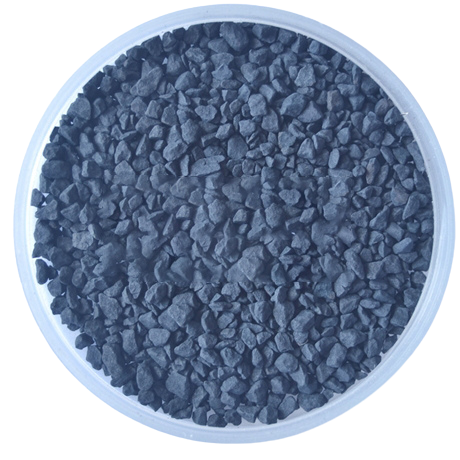
Silicon carbide (SiC) is a wide bandgap semiconductor material with extremely high hardness, thermal stability and excellent electrical conductivity, and is widely used in many high-end fields.
Hardness and wear resistance:
SiC has extremely high hardness, which enables it to withstand the impact of high-energy particles during the film preparation process. The target material needs to have sufficient mechanical strength and wear resistance to ensure that there is no excessive wear or cracking during long-term use.
Thermal stability:
SiC’s high melting point and excellent thermal conductivity enable it to perform well in high-temperature environments. This is particularly suitable for applications in high-power electronic devices and optical film layers. The size and shape of the target material must adapt to the expansion coefficient at high temperatures to ensure stability during the preparation process and the quality of the film.
Electrical conductivity and optical properties:
SiC’s electrical conductivity makes it particularly widely used in the semiconductor field, and its transparent properties also have important applications in optical coatings. This requires the target material to be consistent in size and morphology to ensure the uniformity of the electrical and optical properties of the film.
The size and shape of silicon carbide sputtering targets have a crucial impact on the above characteristics, especially in the specific requirements for target size in the fields of semiconductor devices, high-power electronics, optical films, etc.
Common silicon carbide sputtering target sizes and shapes include round, rectangular and square targets. Different applications require different sizes and shapes:
Usually, the diameter of silicon carbide sputtering targets ranges from 50 mm to 400 mm, and the thickness generally ranges from 5 mm to 20 mm. The standard size depends on the specifications of the sputtering equipment and the deposition requirements.
Circular targets: The most common shape, widely used in the semiconductor field and optical coatings.
Rectangular targets: Used for special equipment or customized production, especially for large-area coating or high-power device requirements.
Square targets: Mostly used for specific experiments or high-efficiency thin film preparation.
The size and shape of the target have a significant impact on the uniformity of the target surface, sputtering efficiency, and the quality of the film. Ensuring the consistency of these size standards is the basis for ensuring film performance and equipment stability.
IC manufacturing: Silicon carbide targets play a key role in the manufacture of high-performance integrated circuits. Its high thermal conductivity and chemical stability make silicon carbide an ideal substrate material, which helps to improve the performance and reliability of integrated circuits.
Power devices: In power electronic devices, the application of silicon carbide sputtering targets can significantly improve the efficiency and temperature resistance of devices. The wide bandgap characteristics of silicon carbide enable it to exhibit excellent performance when operating at high temperatures, high voltages and high frequencies, which is particularly important for energy conversion, automotive and aviation fields.
RF devices: Silicon carbide sputtering targets also play an important role in the manufacture of RF devices. Its excellent electron mobility and thermal stability make silicon carbide an ideal material for the manufacture of high-performance RF devices such as RF power amplifiers and filters.
Solar cells: Silicon carbide sputtering targets show great potential in the manufacture of high-efficiency solar cells. It can not only improve the conversion efficiency of solar cells, but also enhance the durability and stability of cells in extreme environments.
Thin-film solar cells: The application of silicon carbide has also been extended to the production of thin-film solar cells. It can be used as a buffer layer or window layer for thin-film solar cells to improve the performance of the overall cell.
Optical applications: Silicon carbide sputtering targets are widely used in the manufacture of high-performance optical components due to their high refractive index and wear resistance. These components are widely used in aerospace, military and high-precision measuring instruments.
Military and aerospace: The high strength and high temperature resistance of silicon carbide make it used in the manufacture of high-temperature resistant structural components and thermal protection systems in the military and aerospace fields.
Advanced ceramic materials: The high hardness and wear resistance of silicon carbide sputtering targets make them ideal for the production of advanced ceramic materials, which have important applications in the industrial, automotive and energy fields.
Silicon carbide sputtering targets typically range in diameter from 50 mm to 400 mm, and thicknesses generally range from 5 mm to 20 mm. Standard sizes depend on the specifications of the sputtering equipment and deposition requirements.
VI HALBLEITERMATERIAL GmbH (VIMATERIAL) employs a stringent quality assurance system to ensure the reliability of our product quality. Strict quality control is implemented throughout the entire production chain, and for defective products, we strictly enforce the principle of rework and redo. Each batch is released only after passing detailed specification tests.
Every batch of our materials is independently tested, and, if necessary, we send samples to certified companies for testing. We provide these documents and analysis certificates with the shipment to certify that our products meet the required standards.
Contact our team of experts today and let us help you with your business!