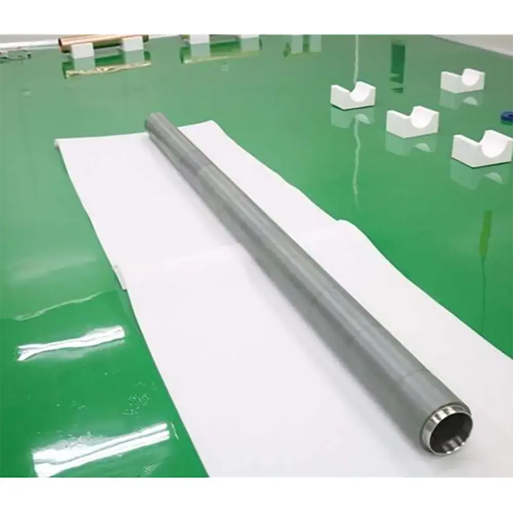
| Product ID | Formula | Purity | Dimension | Quantity | Price in € | Inquiry |
|---|---|---|---|---|---|---|
| 7400ST001 | W | 99.95% | Ø 25.4 mm x 3.175 mm | 1 | POR | Inquire |
| 7400ST002 | W | 99.95% | Ø 25.4 mm x 6.35 mm | 1 | POR | Inquire |
| 7400ST003 | W | 99.95% | Ø 50.8 mm x 3.175 mm | 1 | POR | Inquire |
| 7400ST004 | W | 99.95% | Ø 50.8 mm x 6.35 mm | 1 | POR | Inquire |
| 7400ST005 | W | 99.95% | Ø 76.2 mm x 3.175 mm | 1 | POR | Inquire |
| 7400ST006 | W | 99.95% | Ø 76.2 mm x 6.35 mm | 1 | POR | Inquire |
| 7400ST007 | W | 99.95% | Ø 101.6 mm x 3.175 mm | 1 | POR | Inquire |
| 7400ST008 | W | 99.95% | Ø 101.6 mm x 6.35 mm | 1 | POR | Inquire |
| 7400ST009 | W | 99.95% | 214 mm x 56 mm x 12mm | 1 | POR | Inquire |
| 7400ST010 | W | 99.95% | 764 mm x 131 mm x 14 mm | 1 | POR | Inquire |
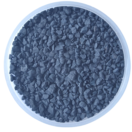
Tungsten metal sputtering target is a kind of tungsten metal, in a high vacuum environment by the ion beam stream bombardment, the surface atoms will be sputtered out and deposited on the surface of the substrate, so as to form a thin film of the key materials, widely used in semiconductors, solar energy, flat-panel displays, and so on many high-tech fields.
Characteristics
Appearance and colour: greyish-white shiny metallic luster.
Atomic weight: The atomic weight of tungsten is 183.84.
Atomic number: the atomic number is 74
Melting point: Tungsten metal has the highest melting point among all pure metals, reaching 3410℃ (6192℉), which makes it still maintain a stable physical state at high temperatures, and can be used in some sputtering coating processes that require high temperatures.
Thermal Conductivity: The thermal conductivity is 174W/m・K, which has good thermal conductivity and can effectively transfer heat during the sputtering process to ensure the uniformity and stability of sputtering.
Coefficient of thermal expansion: The coefficient of thermal expansion is low at 4.5×10-⁶/K, which means that the dimensional change of tungsten sputtering target is small when the temperature changes, which helps to improve the precision and quality of coating.
Theoretical density: The theoretical density of Tungsten metal is as high as 19.25g/cm³, the high density makes the target material have higher atomic number and quality, which can provide more sputtering particles and improve the efficiency and thickness of coating.
Resistance: relatively low resistance, which is conducive to the passage of electric current, and can form a stable electric field during the sputtering process, improving the sputtering efficiency.
Purity and conductivity: High purity tungsten sputtering targets (purity is usually 99.95% and above) have better conductivity, which can reduce the influence of impurities on electron transport, thus improving the electrical properties of the coating.
Hardness: Higher hardness, good abrasion resistance and corrosion resistance, able to maintain good shape and dimensional stability in the sputtering process, prolonging the service life of the target.
Flexural strength: high flexural strength, which makes tungsten sputtering target can withstand certain mechanical stress during installation and use, and is not easy to be deformed and damaged.
Sputtering yield: In the sputtering process, tungsten atoms can be effectively sputtered out to form a high sputtering yield. The size of the sputtering yield is related to the type of sputtering gas, pressure, power and other factors.
Thin Film Characteristics: The thin film formed by sputtering has good adhesion and hardness, and is able to form a uniform, dense film on the substrate with good optical, electrical and mechanical properties.
Applications
Semiconductor field:
Formation of electrodes and wiring: In semiconductor chip manufacturing, tungsten metal sputtering targets can be used to form electrodes and connect wiring inside the chip. As tungsten has good electrical conductivity and high melting point, it can maintain stable electrical performance under high temperature and high current environment to ensure the normal operation of the circuit inside the chip.
Manufacturing diffusion barrier layer: It can be used as a diffusion barrier layer material to prevent mutual diffusion of atoms between different materials and ensure the performance and reliability of semiconductor devices. For example, in the copper interconnect process, tungsten can prevent the diffusion of copper atoms into the surrounding materials, avoiding adverse effects on chip performance.
Making tungsten plug (W-Plug): It is used to fill the gap between the metal layer and the vertical contact holes to achieve the electrical connection between different layers. With the increasing integration of semiconductor chips, the size and performance requirements for tungsten plugs are getting higher and higher, and tungsten sputtering targets are able to meet these high-precision manufacturing needs.
Flat panel display field:
Thin-film transistor (TFT) manufacturing: In flat panel display technologies such as liquid crystal displays (LCD) and organic light-emitting diodes (OLED), tungsten sputtering targets can be used to prepare electrode materials for TFTs, which are the key components of flat panel displays, and whose electrode performance has a direct impact on the quality and response speed of the display. Tungsten electrode has good conductivity and stability, which can improve the performance of TFT.
Transparent conductive film: Through sputtering process on the glass substrate deposition of tungsten oxide film, such as tungsten oxide (WO₃), can be prepared transparent conductive film. This transparent conductive film has both good electrical conductivity and high light transmittance, and is an important material for touch screens, electrodes and other components in flat panel displays.
Solar energy field:
Solar cell electrodes: In the manufacture of solar cells, tungsten metal sputtering targets can be used to prepare electrodes for solar cells. Tungsten electrodes have good electrical conductivity and corrosion resistance, which can improve the conversion efficiency and stability of solar cells. For example, in copper indium gallium selenide (CIGS) solar cells, tungsten can be used as an electrode material to improve cell performance.
Anti-reflective coating: By sputtering a compound film of tungsten, an anti-reflective coating can be prepared on the surface of a solar cell to reduce the reflection loss of light and improve the light absorption efficiency of the solar cell.
Optical field:
Optical Coating: It is used to manufacture various optical films, such as transmittance enhancement film, reflective film, light filtering film and so on. Thin films of tungsten metal have unique optical properties, which can meet the requirements of different optical devices on film performance. For example, in laser technology, tungsten films can be used to prepare high reflective mirrors and laser cavity mirrors to improve laser output power and stability.
Infrared optical devices: tungsten metal has good transmittance and reflectivity in the infrared band, so it can be used to manufacture infrared optical devices, such as infrared windows, infrared lenses and so on. By sputtering tungsten films, the performance and service life of these infrared optical devices can be improved.
Aerospace field:
Coating of high-temperature components: Aerospace equipment operates in high-temperature and high-pressure environments, which requires very high material performance. Tungsten sputtering targets can be used to prepare coatings on the surfaces of high-temperature components such as aero-engine blades and combustion chambers, to improve the components’ high-temperature, corrosion and wear resistance, and to extend their service life.
Satellite components: In spacecraft such as satellites, tungsten metal sputtering targets can be used to manufacture electrodes and wiring for electronic devices, sensors and other components, as well as thermal control coatings on the surface of satellites to ensure the normal operation and reliability of satellites.
Other fields:
Medical equipment: It is used in the manufacture of X-ray tubes in medical equipment, detectors for CT machines and other components. The high density and good X-ray absorption properties of tungsten metal make it an ideal material for key components in these medical devices.
Machining: Depositing tungsten film on the surface of machining tools such as cutting tools and moulds can improve the hardness, wear resistance and corrosion resistance of the tools and extend their service life.
VI HALBLEITERMATERIAL GmbH (VIMATERIAL) employs a stringent quality assurance system to ensure the reliability of our product quality. Strict quality control is implemented throughout the entire production chain, and for defective products, we strictly enforce the principle of rework and redo. Each batch is released only after passing detailed specification tests.
Every batch of our materials is independently tested, and, if necessary, we send samples to certified companies for testing. We provide these documents and analysis certificates with the shipment to certify that our products meet the required standards.
Contact our team of experts today and let us help you with your business!