Zinc Oxide (Ga doped) sputtering target is a kind of semiconductor ceramic sputtering target which is doped with gallium to improve the conductivity, has a hexagonal zinc oxide structure and is transparent in the visible range, and it is mainly used in the fields of electronics and information industry.
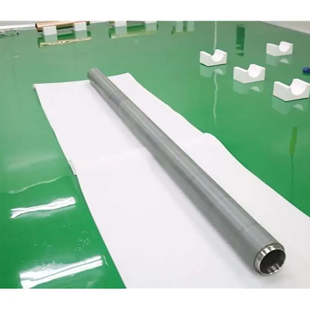
Zinc Oxide sputtering targets doped with 5% gallium have better conductivity and stability than the original targets, and VIMATERIAL produces Zinc Oxide (Ga doped) sputtering targets with 99.9% and 99.99% purity, which are characterized by high purity and excellent product performance. We can also provide binding service, please contact us if you need.
Molecular formula: ZnO-5wt%Ga
Molecular weight: about 81.408g/mol.
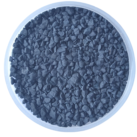
Appearance: Usually white or yellowish target material.
Density: about 5.6g/cm³.
Melting point: about 1975℃.
Boiling point: about 2360°C.
Crystal structure: Hexagonal zincite crystal structure, in which zinc atoms and oxygen atoms are arranged according to a certain law, forming a tetrahedral coordination structure, each zinc atom is surrounded by four oxygen atoms, and each oxygen atom is also surrounded by four zinc atoms, but due to the difference in the radius of the gallium atoms and the zinc atoms, which will lead to small changes in the lattice constant .
|
Composition of 99.9% Zinc Oxide (Ga doped)(wt%) |
||||||||
| ZnO | Ga | Fe | Cu | Ni | Al | Na | Pb | Cd |
| 94.76 | 5.19 | 0.003 | 0.002 | 0.001 | 0.001 | 0.001 | 0.0001 | 0.0001 |
Flat panel display field: used in the manufacture of flat panel displays, can improve the performance of the display device, reduce power consumption, such as the preparation of transparent conductive electrodes in LCD, as anode materials in OLED.
Solar cell field: It is the key material for the preparation of transparent conductive film for thin film solar cell and heterojunction solar cell, which can improve the photoelectric conversion efficiency of the cell.
Electronic devices: used as semiconductor materials for integrated circuits, such as gate materials for MOSFETs or insulating layer materials, etc., to regulate electron transport and device electrical properties.
Optical device field: it can be used to prepare transparent conductive layer for optical sensors, touch screen and other devices, using its good conductivity and visible light transparency to realize signal transmission and touch sensing function.
Each batch of products will be inspected for composition, microstructure, binding strength, size and other characteristics and issue inspection reports, and will also provide samples for customers to re-inspect.
We use vacuum bagging, double vacuum bagging, and for special targets, we also use boxed packaging for protection.
ZnO – 5wt% Ga targets should be stored in a dry, cool, well-ventilated environment to avoid moisture, oxidation, and to prevent contact with corrosive substances, and at the same time be careful to avoid physical collision and violent vibration, and need to stay away from high temperatures and strong light irradiation to maintain the stability of its physical and chemical properties.
VI HALBLEITERMATERIAL GmbH (VIMATERIAL) employs a stringent quality assurance system to ensure the reliability of our product quality. Strict quality control is implemented throughout the entire production chain, and for defective products, we strictly enforce the principle of rework and redo. Each batch is released only after passing detailed specification tests.
Every batch of our materials is independently tested, and, if necessary, we send samples to certified companies for testing. We provide these documents and analysis certificates with the shipment to certify that our products meet the required standards.
Contact our team of experts today and let us help you with your business!