| Product ID | Formula | Purity | Dimension | Quantity | Price in € | Inquiry |
|---|---|---|---|---|---|---|
| 1400WF001 | Si | 99.99% | Ø 50.8mm x 0.1 mm th. | 1 | POR | Inquire |
| 1400WF003 | Si | 99.99% | Ø 101.6mm x 0.2 mm th. | 1 | POR | Inquire |
| 1400WF002 | Si | 99.99% | Ø 50.8mm x 0.675 mm th. | 1 | POR | Inquire |
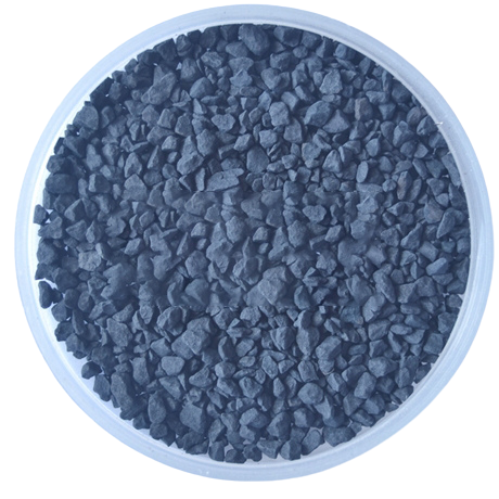
Silicon wafers are particularly useful in manufacturing electronic circuits as substrates for chips. Silicon ranks seventh as the most common element in the entire universe and the second most common element on Earth. Silicon is currently the most widely used semiconductor in semiconductor technology.
Silicon wafers come in a variety of shapes and sizes, depending on their purpose. Wafers range from 2 inches to 12 inches, with 6 inches, 8 inches, and 12 inches being the most common.
VIMATERIAL can provide high-quality single crystal silicon wafers of various specifications, as well as single crystal silicon wafer processing and customization services.
Silicon (through reduction)–>Metallic silicon (through purification)–>Polycrystalline silicon (through heating and melting in a crucible)–>Molten silicon (through Czochralski method)–>Single crystal silicon rod (through wire knife cutting)–>Silicon wafer (through chemical mechanical grinding)–>Polished wafer (through heat treatment)–>Annealed wafer (through epitaxial growth)–>Epitaxial wafer (through a variety of processes)–>Manufacturing various integrated circuits or discrete devices
VI HALBLEITERMATERIAL GmbH (VIMATERIAL) employs a stringent quality assurance system to ensure the reliability of our product quality. Strict quality control is implemented throughout the entire production chain, and for defective products, we strictly enforce the principle of rework and redo. Each batch is released only after passing detailed specification tests.
Every batch of our materials is independently tested, and, if necessary, we send samples to certified companies for testing. We provide these documents and analysis certificates with the shipment to certify that our products meet the required standards.
Contact our team of experts today and let us help you with your business!