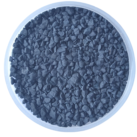
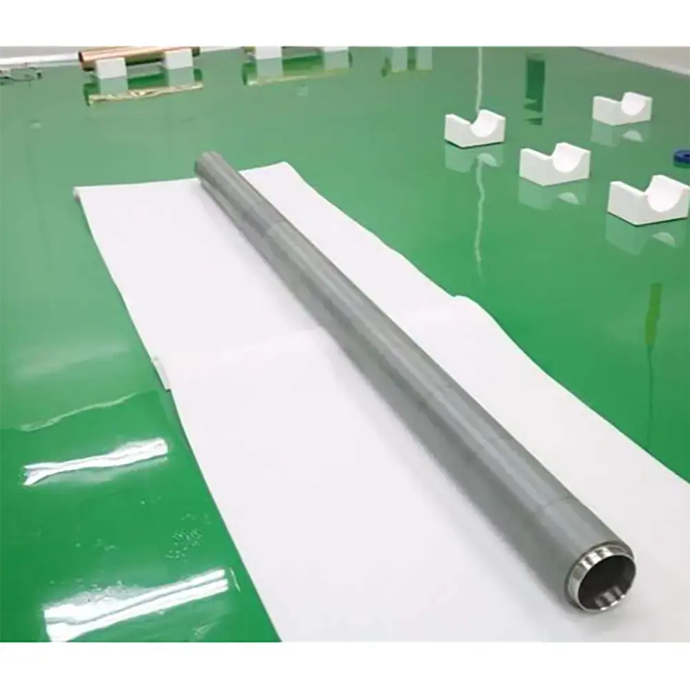
Niobium Selenide sputtering target is a ceramic compound target composed of niobium and selenium with a specific crystal structure and excellent properties, which can be used for the preparation of thin films with lubricating, conductive and superconducting properties by sputter coating technology.
Properties
Chemical formula and composition: The chemical formula is NbSe₂, which consists of two elements, niobium (Nb) and selenium (Se).
Crystal structure: Layered hexagonal crystal structure, this structure makes it show unique advantages in lubrication, electrical and other properties, laying the foundation for its application in different fields.
Stability: Chemical stability is good at room temperature and pressure, but chemical reactions may occur at high temperatures, strong oxidizing or reducing environments, so attention should be paid to environmental conditions during use and storage.
Applications
Electronic devices: It can be used to prepare electrodes, contact layers, and superconducting films for semiconductor devices, integrated circuits, and so on. For example, Niobium Selenide’s superconducting properties make it potentially useful in high-performance electronic devices such as superconducting quantum bits and superconducting sensors, which can improve the performance and operating speed of the devices.
Lubrication field: because it has a layered shear structure similar to MoS₂, with excellent lubrication properties, while showing metal conductivity, is a combination of lubrication and conductivity of the material can be used to prepare a variety of lubrication and conductivity of the components, such as motor brushes, special bearings, wire-wound potentiometer contacts.
Photovoltaic field: can be used to prepare the absorption layer or buffer layer in photovoltaic cells, through the sputtering coating technology will be NbSe₂ and other materials deposited on the substrate, the formation of a thin film with specific properties, which can help to improve the photovoltaic cell photoelectric conversion efficiency and stability.
Optoelectronic devices: such as photodetectors, light-emitting diodes, etc., Niobium Selenide sputtering target preparation of thin films can regulate the optical and electrical properties of optoelectronic devices, to achieve high efficiency of light absorption, emission and detection, to expand the scope of application and performance of optoelectronic devices.