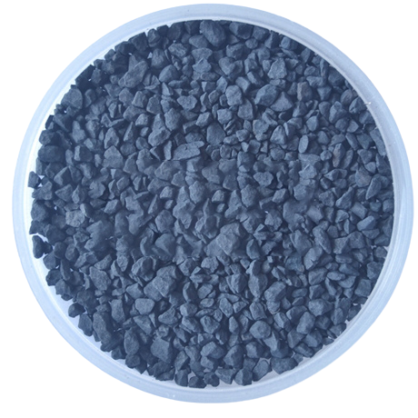
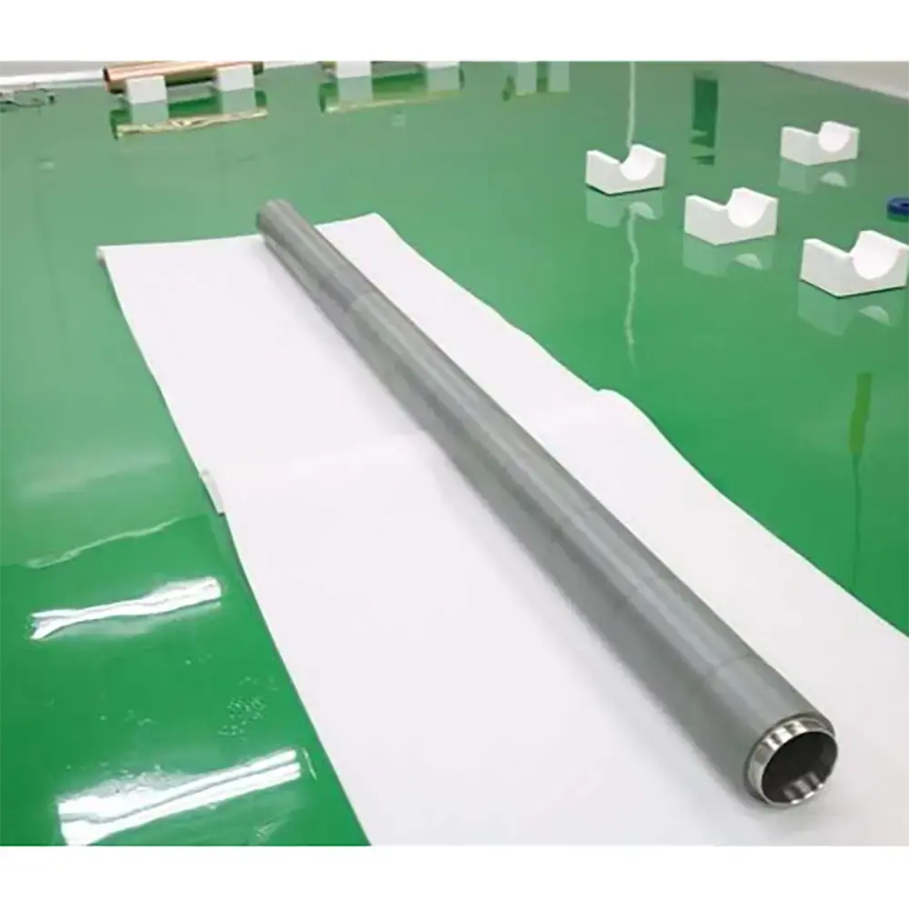
Niobium Boride sputtering targets are made of niobium boride with high hardness, high melting point, good electrical and thermal conductivity and chemical stability, etc. They are prepared by powder metallurgy and are used as important sputtering coating materials for electronic devices, hard coatings and other applications.
Properties
Density: The density of niobium boride is about 6.97g/ml (25℃), and the relative density (15.5℃) is 7.00, the higher density enables it to better maintain the shape and structural stability during the sputtering process.
Melting point: up to 3000℃-3050℃, with excellent high temperature resistance, can be stable in high temperature sputtering environment, not easy to melt or deformation, to ensure the smooth progress of sputtering process.
Hardness: the hardness is about 2600kg/mm², this high hardness characteristic makes the sputtering target material not easy to produce deformation and abrasion under ion bombardment, which is conducive to ensuring the uniformity and quality stability of sputtered films, and at the same time, makes the prepared films have good abrasion resistance.
Lattice Constants: Niobium boride has lattice constants a=0.310nm, c=0.330nm, and its specific lattice structure affects the arrangement of atoms and the growth of the film during the sputtering process, which in turn affects the properties of the film.
Chemical properties: at room temperature, it has good stability to most chemical substances and is not easy to be corroded, which makes the sputtering target have a long life in the storage and use process, and the prepared film also has a certain degree of chemical stability, which can be used in some environments that require chemical stability.
Electrical properties: good electrical conductivity, can effectively transmit the current in the sputtering process, produce a stable plasma, and help to improve the sputtering efficiency and film quality.
Microstructure: The microstructure includes grain size, grain boundaries, etc. A uniform and fine grain structure helps to improve the target’s densification and sputtering performance, reduces the generation of particles in the sputtering process, and thus improves the quality and uniformity of the film.
Applications
Electronic devices: In integrated circuit manufacturing, it can be used to deposit niobium boride film as diffusion barrier layer, metal interconnect layer, etc. It can improve the performance and reliability of electronic devices, prevent the diffusion of metal atoms, and ensure the stable transmission of electronic signals. At the same time, its good conductivity also helps to reduce the resistance of electronic devices and improve their efficiency.
Hard coating: niobium boride can be used to prepare niobium boride hard coating on the surface of cutting tools, molds and other mechanical parts, which significantly improves the hardness, wear resistance and service life of the parts, reduces the wear and tear of cutting tools and deformation of molds, and improves the machining accuracy and productivity, and it is widely used in the fields of machining, automobile manufacturing, and aerospace.
Optical thin film: Through sputtering coating process, niobium boride thin film can be prepared on the surface of optical components, which can be used to adjust the reflectivity, transmittance and other optical properties of the optical components, and to manufacture high-performance optical filters, mirrors and other optical devices to meet the high-performance requirements for optical thin film in the fields of optical communications, laser technology, optical instruments and so on.
Superconducting materials: part of niobium boride has superconducting properties, so niobium boride sputtering targets also have certain application prospects in the field of superconductivity, which can be used to prepare superconducting thin films, research and development of new superconducting materials and superconducting devices, and to provide basic material support for the fields of energy storage, quantum computation and so on.
VI HALBLEITERMATERIAL GmbH (VIMATERIAL) employs a stringent quality assurance system to ensure the reliability of our product quality. Strict quality control is implemented throughout the entire production chain, and for defective products, we strictly enforce the principle of rework and redo. Each batch is released only after passing detailed specification tests.
Every batch of our materials is independently tested, and, if necessary, we send samples to certified companies for testing. We provide these documents and analysis certificates with the shipment to certify that our products meet the required standards.
Contact our team of experts today and let us help you with your business!