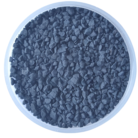
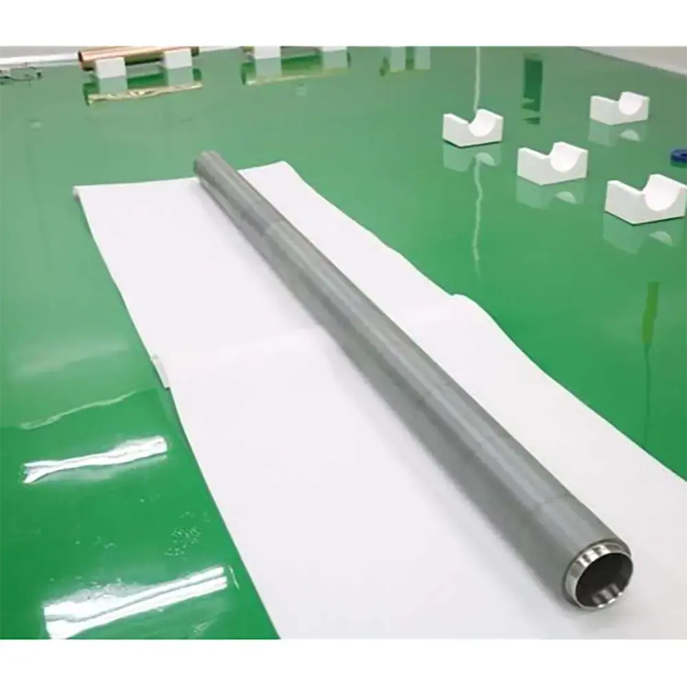
Molybdenum Tantalum Alloy Sputtering Targets are sputtering targets made of an alloy of two metals, molybdenum and tantalum, used to deposit thin films of molybdenum tantalum alloy on a substrate by a sputtering process.
Characteristics
Density: Molybdenum Tantalum alloy has a high density, which varies depending on the ratio of molybdenum to tantalum and the preparation process, but is generally higher than the density of a simple mixture of its constituent elements, which is favourable for the uniform sputtering of atoms during ion bombardment to form a homogeneous thin film.
Melting point: Molybdenum has a melting point of about 2623°C and Tantalum has a melting point of about 3017°C. The melting point of the alloys is also maintained at a high level, so that they can maintain a stable physical state at high temperatures, which ensures that they can provide a stable supply of atoms during high-temperature sputtering to ensure uniformity and consistency of the thin film deposition.
Vapour Pressure: Low vapour pressure in a vacuum environment, non-volatile, ensures stable deposition of target components on the substrate during the sputtering process, ensuring the accuracy and stability of the film composition.
Resistivity: The range of resistivity depends on the ratio of molybdenum and tantalum and the preparation process, etc. Generally speaking, the resistivity of molybdenum is about 5.2×10-⁸Ω・m, and the resistivity of tantalum is about 12.45×10-⁸Ω・m, and the resistivity of tantalum is about 12.45×10-⁸Ω・m, which can be adjusted to meet the requirements of different applications. The resistivity can be adjusted to meet the requirements of conductivity in different application scenarios.
Grain size: the average grain size is usually small, generally in the micron level or even smaller, the fine grain structure can improve the density and uniformity of sputtered films, improve the mechanical properties, electrical properties and corrosion resistance of the film, and at the same time, reduce the surface roughness of the film, improve the optical properties and surface quality.
Applications
Electronics and Semiconductors
Semiconductor chip manufacturing: Molybdenum Tantalum Alloy can be used to deposit metal films in semiconductor wafer manufacturing, such as as a barrier layer, contact layer and so on. For example, in copper interconnect technology, tantalum is one of the important materials, and molybdenum tantalum alloy sputtering target can provide better performance and adaptability, which can help improve the performance and reliability of semiconductor chips, and meet the requirements of chip manufacturing for high-precision and high-performance materials.
Integrated Circuit: It is one of the core materials for the preparation of integrated circuits, and can be used for the manufacture of various electronic components, such as transistors and capacitors. Its high purity and good uniformity can ensure the formation of high-quality conductive layer, insulating layer, etc. in integrated circuits, thus improving the performance and stability of integrated circuits, which is important for achieving smaller chip size, higher integration and faster operation speed.
Display technology field
Flat panel displays: In flat panel display technologies such as liquid crystal displays (LCDs) and organic light-emitting diode displays (OLEDs), the sputtering target can be used to prepare transparent conductive films, electrodes, and other components. For example, the molybdenum tantalum alloy film formed by sputtering deposition can be used as the anode material in OLED displays with good conductivity and stability, which can effectively improve the luminous efficiency and service life of the display, and at the same time, it can also be achieved to achieve a narrower bezel design and improve the screen-to-body ratio.
Display panel manufacturing: Molybdenum Tantalum Alloy helps to improve the uniformity of the large-area film layer in the display panel, ensuring the colour uniformity and brightness consistency of the display screen. During the manufacturing process, the thickness and performance of the film can be precisely controlled, thus improving the overall quality and display effect of the display panel, and meeting the requirements of high-resolution, high-contrast displays.
Photovoltaic field
Can be used in the preparation of thin film solar cells, compared with the traditional crystalline silicon solar cells, thin film solar cells using the sputtering target can greatly reduce the amount of material, thereby significantly reducing the manufacturing costs and product prices, but also has a low manufacturing temperature, a wide range of applications, etc., in the integration of photovoltaic buildings, large-scale, low-cost power plant construction, etc., than the traditional crystalline silicon solar cells have a much broader market space. Wide market space, with the carbon neutral, carbon peak target put forward, photovoltaic installed capacity to enhance the certainty of strong, its application in the field of photovoltaic market will grow steadily.
Data Storage
In the manufacture of data storage devices such as hard discs and optical discs, magnetic films or other functional films can be deposited. For example, in the field of high-density hard discs, magnetic films are almost always made by sputtering, and molybdenum tantalum alloy sputtering targets are able to meet the requirements for high purity, low gas content, fine grain microstructure, uniform metallurgy, high magnetic penetration and usage, and excellent electrical and mechanical properties, thereby improving the density and reliability of data storage.
VI HALBLEITERMATERIAL GmbH (VIMATERIAL) employs a stringent quality assurance system to ensure the reliability of our product quality. Strict quality control is implemented throughout the entire production chain, and for defective products, we strictly enforce the principle of rework and redo. Each batch is released only after passing detailed specification tests.
Every batch of our materials is independently tested, and, if necessary, we send samples to certified companies for testing. We provide these documents and analysis certificates with the shipment to certify that our products meet the required standards.
Contact our team of experts today and let us help you with your business!