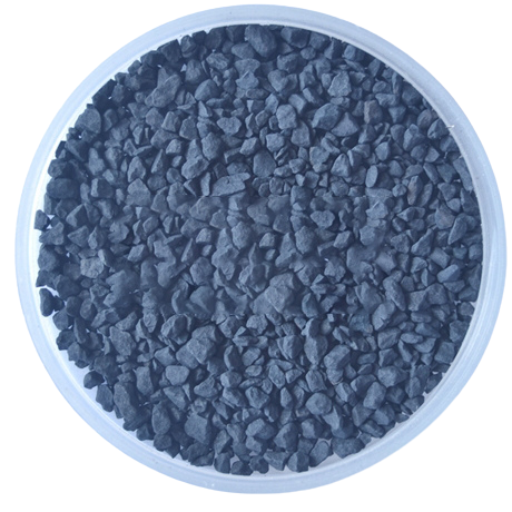
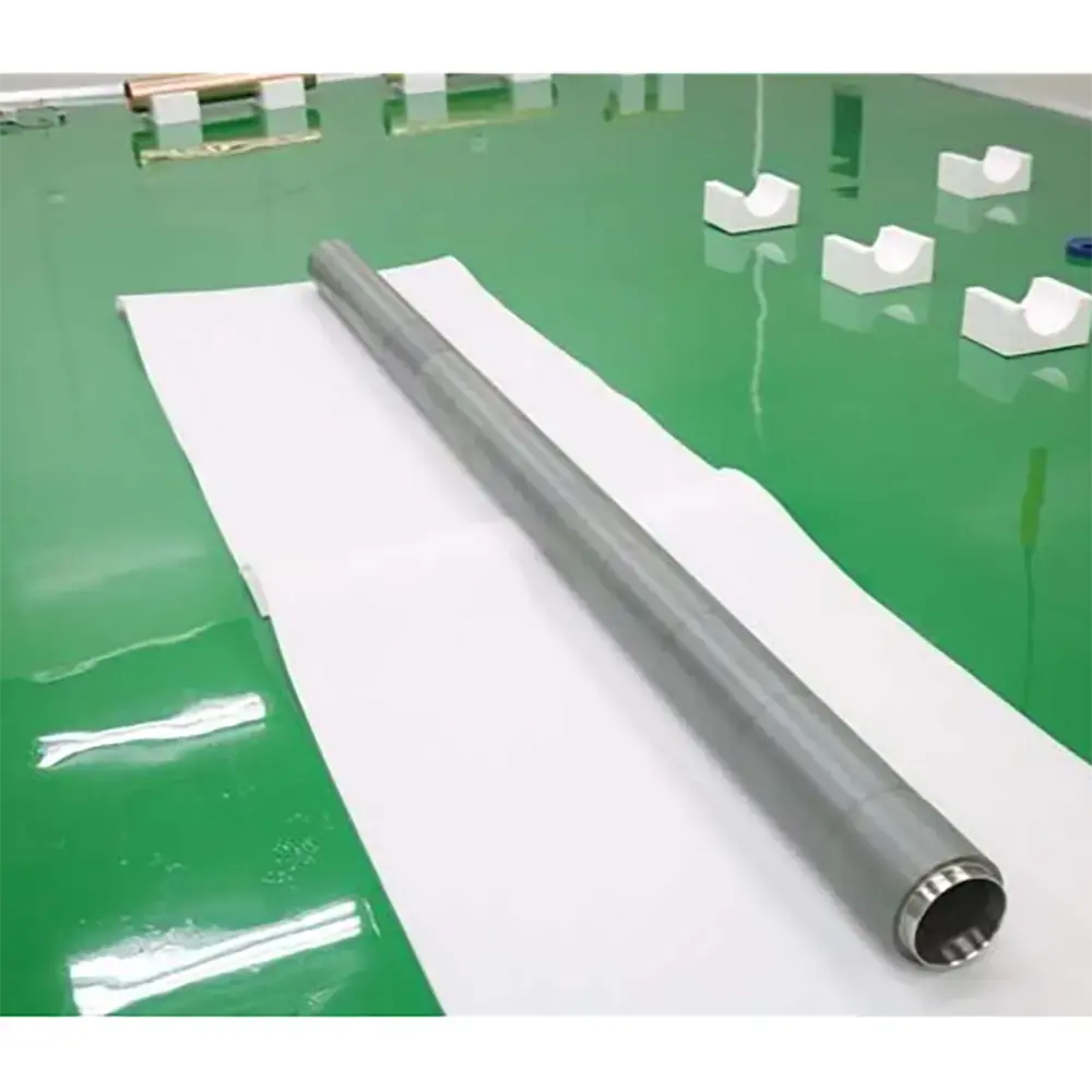
Molybdenum Silicon Alloy sputtering target is an alloy material composed of molybdenum and silicon, with good electrical conductivity, high hardness, suitable melting point and thermal conductivity and other physical properties, through the sputtering process can be in the semiconductor, flat panel display, solar photovoltaic, optical coating and many other fields to deposit high-quality thin films used for electrical conductivity, barrier, encapsulation, optical coating and other applications. Applications.
Properties
Density: Molybdenum has a density of approx. 10.2 g/cm3 and silicon 2.33 g/cm3. Molybdenum-silicon alloy sputtering targets have an in-between density, usually around 6-8 g/cm3, but the exact value varies depending on the ratio of molybdenum to silicon.
Hardness: Molybdenum has a high hardness and the addition of silicon further increases the hardness of the alloy, usually between 7 and 9 on the Mohs hardness scale, which allows the target to maintain good shape stability during sputtering and reduces wear and deformation.
Melting point: The melting point of pure molybdenum is about 2620°C, the melting point of silicon is about 1414°C, and the melting point of molybdenum-silicon alloys is generally between 1800°C and 2200°C. The specific melting point depends on the compositional ratio of the alloy.
Thermal conductivity: Molybdenum has a good thermal conductivity, the thermal conductivity of pure molybdenum is about 138 Watt/(metre/kelvin), the thermal conductivity of silicon is relatively low. The thermal conductivity of molybdenum-silicon sputtering targets is influenced by the composition ratio and microstructure, and is generally in the range of 80-120 W/(m/km).
Applications
Semiconductor industry: In semiconductor manufacturing, molybdenum silicon alloy sputtering targets can be used to prepare electrodes, wiring and other structures for devices such as thin-film transistors (TFTs) and integrated circuits (ICs). For example, in TFT-LCD (thin-film transistor liquid crystal display), molybdenum-silicon alloy thin film can be used as the conductive material of gate and source-drain electrodes, which has good conductivity and stability, and can meet the high-performance requirements of semiconductor devices.
Solar Cells: Used in the preparation of components such as electrodes and reflective layers for solar cells. Molybdenum silicon alloy film has good photoelectric properties and stability, which can improve the conversion efficiency and service life of solar cells.
Flat panel display industry: In flat panel display technology, such as OLED (Organic Light Emitting Diode) and QLED (Quantum Dot Light Emitting Diode) displays, molybdenum silicon alloy sputtering targets can be used for the preparation of electrodes and wiring and other structures of the display panels, providing stable electrical properties for the display panels.
Coating field: Functional coatings can be prepared on the surface of some parts, such as wear-resistant coatings and corrosion-resistant coatings. Molybdenum silicon alloy coating has high hardness and good corrosion resistance, which can improve the service life and performance of parts.
VI HALBLEITERMATERIAL GmbH (VIMATERIAL) employs a stringent quality assurance system to ensure the reliability of our product quality. Strict quality control is implemented throughout the entire production chain, and for defective products, we strictly enforce the principle of rework and redo. Each batch is released only after passing detailed specification tests.
Every batch of our materials is independently tested, and, if necessary, we send samples to certified companies for testing. We provide these documents and analysis certificates with the shipment to certify that our products meet the required standards.
Contact our team of experts today and let us help you with your business!