Molybdenum Selenide sputtering target is a material with characteristics such as high purity and high density, which is suitable for sputter coating technology and has important applications in many fields such as semiconductors, display technology and photovoltaics.
Characteristics
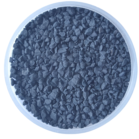
Appearance and morphology: Usually grey powder with a layered structure.
Density: Density about 6.0 g/ml.
Melting point: melting point about 1200°C.
Hardness: low on the Mohs hardness scale, relatively soft.
Semiconductor properties: semiconductor properties, its electrical properties can be adjusted by doping and other means, in the field of electronic devices and other important applications.
Optical properties: the absorption and emission of light has certain characteristics, in optoelectronic devices and other aspects of potential applications, such as molybdenum selenide quantum dots can be used in light-emitting diodes and other devices.
Stability: relatively stable chemical properties, but under certain conditions will also occur chemical reactions .
Oxidising: easily oxidised in air and at high temperatures to produce the corresponding oxides.
Acid-base: insoluble in water and common acid-base solutions, but soluble in some strong oxidising acids, such as hot sulphuric acid, aqua regia, etc. .
Reaction with metals: it can react with some metals to form alloys or intermetallic compounds, thus changing the properties of the materials, and can be used to prepare composite materials with specific properties.
Applications
Semiconductor field: Molybdenum Selenide is one of the key materials for the preparation of semiconductor devices, and can be used for the deposition of semiconductor thin films, such as in the wafer fabrication process, through the sputtering coating technology, Molybdenum Selenide target atoms deposited on the surface of the wafer to form semiconductor thin films with specific electrical properties, and the thickness and composition of the film can be precisely controlled, so as to achieve the performance of semiconductor devices. The thickness and composition of the film can be accurately controlled to achieve the regulation of semiconductor device performance to meet the needs of different application scenarios.
Display Technology: It plays an important role in the flat panel display industry, such as liquid crystal display (LCD), organic light-emitting diode display (OLED) and other technologies. OLED, for example, Molybdenum Selenide sputtering target can be used to prepare the cathode material in the device, which helps to achieve the effective injection of electrons, improve the luminous efficiency and service life of the display device; in LCD, it can be used in the preparation of thin film transistor arrays and other components, to ensure that the uniformity of the large-area film layer to enhance the quality and performance of the display.
Photovoltaic field: Molybdenum Selenide can be used in the preparation of thin film solar cells, especially in heterojunction cells, for the deposition of transparent conductive film and other functional layers. Heterojunction battery transparent conductive film deposition process requires the use of a large number of sputtering targets to deposit the formation of TCO transparent metal oxide conductive film, Molybdenum Selenide sputtering target to meet this demand, help to improve the photoelectric conversion efficiency and stability of the battery, with the rapid expansion of heterojunction battery production capacity in the future, the application of its application in the field of photovoltaic is promising.
Optical Coating: It can be used to prepare various kinds of optical films, such as transmittance enhancement film, reflective film, light filtering film and so on. By adjusting the sputtering process parameters and film thickness, it can achieve precise control of light reflection, transmission, absorption and other characteristics, so as to meet the performance requirements of different optical systems, such as in optical lenses, optical instruments, optical communication devices and other products are used to improve optical performance and system efficiency.
Electronic devices: Molybdenum Selenide can be used in the preparation of various functional films in electronic devices, such as electrode films, insulating films, magnetic films and so on. For example, in the manufacture of capacitors, resistors, inductors and other electronic components, the use of sputtering coating technology to deposit the corresponding thin film material to achieve the specific electrical properties of the components; in the magnetic recording devices, can be used to prepare magnetic films to improve the storage density and read-write performance.
Wear-resistant materials: the prepared film has good wear resistance and lubrication properties, and can be applied to the surface treatment of mechanical parts, such as the deposition of Molybdenum Selenide film on the surface of cutting tools, moulds, bearings and other components, which can reduce the coefficient of friction, reduce wear and tear, improve the service life of the components and work efficiency, and reduce the cost of maintenance of equipment.
High-temperature corrosion-resistant field: The thin film formed by the sputtering target has good chemical stability and antioxidant performance under high-temperature environment, which can be used to protect metal materials from high-temperature oxidation and corrosion. For example, it can be used to prepare protective films on the surface of high-temperature components in aerospace, energy and power fields to improve the reliability and durability of the components and extend their service life.
High-grade decorative products field: can be used in glass, ceramics, plastics and other materials on the surface of the preparation of metal luster and decorative effect of the film, such as watch dials, mobile phone shells, jewellery and other products on the decorative coating, not only to improve the aesthetics and added value of the product, but also to give it a certain functionality, such as abrasion, corrosion and so on.
VI HALBLEITERMATERIAL GmbH (VIMATERIAL) employs a stringent quality assurance system to ensure the reliability of our product quality. Strict quality control is implemented throughout the entire production chain, and for defective products, we strictly enforce the principle of rework and redo. Each batch is released only after passing detailed specification tests.
Every batch of our materials is independently tested, and, if necessary, we send samples to certified companies for testing. We provide these documents and analysis certificates with the shipment to certify that our products meet the required standards.
Contact our team of experts today and let us help you with your business!