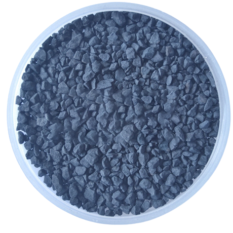
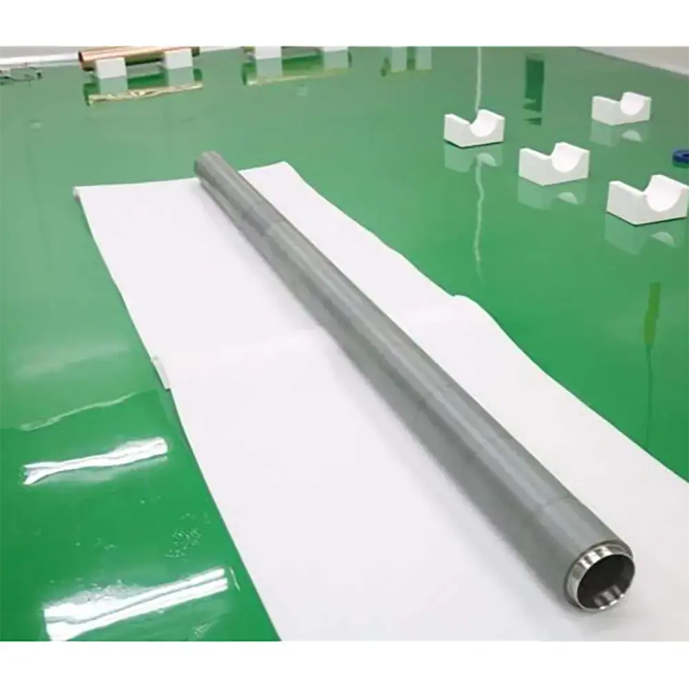
Gallium Selenide sputtering target is a material for physical vapor deposition consisting of gallium and selenium with hexagonal crystal structure, good physical and optical properties, obtained by various preparation methods, and plays a key role in semiconductors, optics, solar cells and flat panel displays.
Properties
Physical properties: relatively high density, which helps to maintain the stability of the target material during sputtering, reducing vibration and displacement during sputtering; relatively high melting point of about 937 ℃ or less can be maintained in a solid state at higher temperatures under the sputtering environment to ensure that the sputtering is carried out properly; the color is usually brown or black.
Optical properties: GaS sputtering targets have a strong photoluminescent direct band gap of about 2eV, which makes GaS sputtering targets have a wide range of applications in the field of optics, for example, it can be used in the preparation of optical films, light-emitting devices, and so on.
Electrical properties: As a semiconductor material, it has certain electrical conductivity and electron transport properties, which are very important for the preparation of thin film layers for electronic devices.
Applications
Semiconductor field: In the manufacture of semiconductor devices, gallium selenide sputtering targets are used to prepare thin film layers for devices such as thin-film transistors (TFTs) and integrated circuits (ICs). For example, by sputtering gallium selenide thin films, conductive, insulating, or semiconductor layers can be formed on semiconductor chips, thereby realizing various functions of the device.
Optical field: Due to its unique optical properties, it can be used to prepare optical films, such as transmittance enhancement films, reflective films, and filter films. These optical films are widely used in optical instruments, optical sensors, laser devices and other fields. In addition, gallium selenide can also be used to prepare light-emitting diodes (LED), lasers and other optoelectronic devices, which can improve the luminous efficiency and performance of the device.
Solar cell field: In the manufacture of solar cells, gallium selenide sputtering targets can be used to prepare the absorption layer or window layer of solar cells. Gallium selenide has a moderate bandgap width, can effectively absorb sunlight, and has a high photoelectric conversion efficiency, so it can improve the performance of solar cells.
Other fields: Gallium selenide sputtering targets are also used in flat panel display, magnetic recording, sensors and other fields. For example, in flat panel display, it can be used for the preparation of liquid crystal display (LCD) electrode materials; in magnetic recording, it can be used for the preparation of thin film layer of magnetic recording medium; in sensors, it can be used for the preparation of thin film layer of sensitive components.
VI HALBLEITERMATERIAL GmbH (VIMATERIAL) employs a stringent quality assurance system to ensure the reliability of our product quality. Strict quality control is implemented throughout the entire production chain, and for defective products, we strictly enforce the principle of rework and redo. Each batch is released only after passing detailed specification tests.
Every batch of our materials is independently tested, and, if necessary, we send samples to certified companies for testing. We provide these documents and analysis certificates with the shipment to certify that our products meet the required standards.
Contact our team of experts today and let us help you with your business!