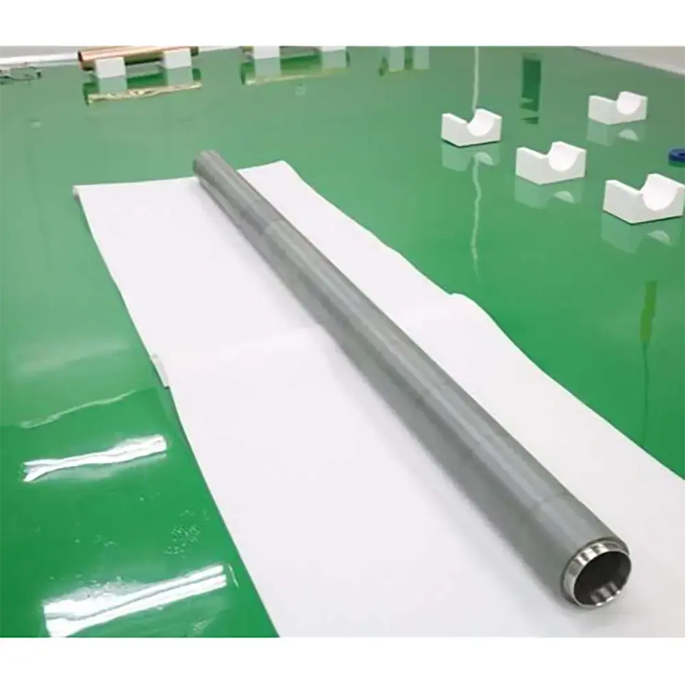
| Product ID | Formula | Purity | Dimension | Quantity | Price in € | Inquiry |
|---|---|---|---|---|---|---|
| 311500ST001 | GaP | 99.999% | Ø 50.8 mm x 3.175 mm | 1 | POR | Inquire |
| 311500ST002 | GaP | 99.999% | Ø 50.8 mm x 6.35 mm | 1 | POR | Inquire |
| 311500ST003 | GaP | 99.999% | Ø 76.2 mm x 3.175 mm | 1 | POR | Inquire |
| 311500ST004 | GaP | 99.999% | Ø 101.6 mm x 3.175 mm | 1 | POR | Inquire |
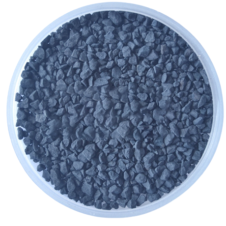
Gallium Phosphide sputtering target is a kind of important semiconductor material sputtering target with high purity, good crystallization, high density, low porosity and excellent thermal conductivity, etc. It is prepared by powder metallurgy or melting casting method, and is widely used in optoelectronic devices, integrated circuits, photovoltaic field and sensors.
Characteristics
Chemical formula: GaP
Molecular weight: 100.697
Good crystalline properties: Good crystal structure and crystallinity, with uniform grain size and orientation, are conducive to the formation of high-quality, uniform films during the sputtering process, thus improving the performance and consistency of semiconductor devices.
High density and low porosity: High-density targets can improve the atomic utilization rate in the sputtering process and reduce particle splashing and target loss in the sputtering process. At the same time, low porosity ensures the stability of the target material during sputtering, preventing problems such as uneven sputtering or target rupture due to the presence of pores.
Excellent thermal conductivity: In the sputtering process, the target absorbs a large amount of heat, and good thermal conductivity helps the rapid dispersion of heat, preventing the target from deformation and melting due to local overheating, thus ensuring the stability of the sputtering process and improving the service life of the target and the quality of the sputtered film.
Applications
Optoelectronic devices: In the manufacture of light-emitting diodes (LEDs), laser diodes (LDs) and other optoelectronic devices, Gallium Phosphide sputtering targets are widely used in the preparation of active layers, limiting layers, ohmic contact layers and other key thin-film structures in the devices. It can improve the luminous efficiency, wavelength stability and reliability of optoelectronic devices, thus promoting the development of optical communication, display technology, lighting and other fields.
Integrated circuits: With the continuous development of integrated circuit technology, the demand for high-performance semiconductor materials is increasing. Gallium Phosphide sputtering targets can be used to manufacture high-frequency, high-speed, high-power transistors and interconnections in integrated circuits, barrier layers and other structures, which helps to increase the operating speed of integrated circuits, reduce power consumption and improve the degree of integration, to meet the requirements of modern electronic equipment for high-performance and miniaturization. The structure of transistors and interconnections in integrated circuits helps to increase the operating speed of integrated circuits, reduce power consumption and improve integration, meeting the requirements of modern electronic equipment for high performance and miniaturization.
Photovoltaic field: In the research and development of solar cells, Gallium Phosphide materials have attracted attention because of their suitable bandwidth and good photoelectric conversion performance, Gallium Phosphide sputtering targets can be used for the preparation of absorber layer, window layer, and other key components of solar cells, which is expected to improve the photoelectric conversion efficiency of solar cells, and provide support for the development of renewable energy. Supporting the development of renewable energy.
Sensors: Gallium Phosphide is sensitive to certain gases, biomolecules and other substances, and can be used to manufacture high-performance gas sensors, biosensors and so on. Gallium Phosphide film is deposited on the sensor substrate by sputtering technology. When the sensor comes into contact with the target substance, the electrical properties of the film will change, thus realizing the detection and monitoring of the target substance.
VI HALBLEITERMATERIAL GmbH (VIMATERIAL) employs a stringent quality assurance system to ensure the reliability of our product quality. Strict quality control is implemented throughout the entire production chain, and for defective products, we strictly enforce the principle of rework and redo. Each batch is released only after passing detailed specification tests.
Every batch of our materials is independently tested, and, if necessary, we send samples to certified companies for testing. We provide these documents and analysis certificates with the shipment to certify that our products meet the required standards.
Contact our team of experts today and let us help you with your business!