Gallium Arsenide wafer is a circular wafer made of Gallium Arsenide material with high electron mobility, high saturation electron rate, direct bandgap, etc. It is a semiconductor material that has a wide range of applications in the fields of RF devices, optoelectronic devices and solar cells.
Characteristics
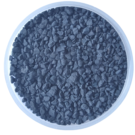
Appearance: usually black and gray cubic crystal system sphalerite crystals, odorless.
Density: relatively high density, about 5.31 – 5.32 g/cm³, which makes the wafers have a certain weight and stability, in the processing and use of the process need to pay attention to its weight on the equipment and process.
Melting point: high melting point, about 1238 ℃, which means that in the high-temperature environment of gallium arsenide wafers have good stability, but in the processing process requires higher temperatures in order to make it melt or related heat treatment.
High electron mobility: electron mobility is 5 – 6 times greater than silicon, which gives GaAs wafers a significant advantage in the manufacture of high-frequency, high-speed electronic devices, enabling fast electronic transmission and response, suitable for microwave devices, high-speed digital circuits and so on.
Semi-insulating: It can be made into semi-insulating high-resistance material with resistivity more than 3 orders of magnitude higher than silicon and germanium. This characteristic enables it to be used as a substrate material in integrated circuits to provide good insulation and reduce leakage and signal interference in circuits.
Suitable forbidden bandwidth: With a forbidden bandwidth of about 1.424 eV (electron volts), it is a direct bandgap semiconductor material. The direct bandgap characteristic makes Gallium Arsenide have high luminous efficiency in optoelectronic devices, which is very suitable for manufacturing light-emitting diodes, laser diodes and other optoelectronic devices.
Optical properties: good absorption and emission performance of light, high optical transmittance and refractive index in the infrared and visible range, can effectively absorb and emit photons, so there are a wide range of applications in the field of optical communications, optical imaging and other fields.
Other characteristics: GaAs wafers also have higher breakdown electric field, higher saturation electron velocity and other characteristics, so that it has a better performance in high-power, high-frequency applications. At the same time, it can be stabilized in air at 600℃ or less, and is not eroded by non-oxidizing acids, but will decompose at high temperatures.
Applications
Electronic device field:
Microwave devices: widely used in microwave frequency circuits, such as microwave power amplifiers, low noise amplifiers, mixers, etc.. Its high electron mobility and low noise characteristics make gallium arsenide microwave devices in radar, satellite communications, wireless communications and other high-frequency communication systems have important applications, to achieve high-frequency, high-power signal transmission and processing.
High-speed digital circuits: Due to the high-speed electronic transmission characteristics, it can be used to manufacture high-speed digital integrated circuits, such as high-speed processors, high-speed memory, etc., which can improve the circuit’s operating speed and processing capacity.
Field Effect Transistor (FET): GaAs FET has the advantages of high input impedance, low noise, high frequency response, etc. It plays an important role in signal amplification and switching control of electronic devices.
Optoelectronic device field:
Light Emitting Diode (LED): Gallium Arsenide is an important material in the manufacture of high brightness and high efficiency light emitting diodes, which emit light covering the range from infrared to visible light, and can be used in a variety of applications such as illumination, display, and indicator lights.
Laser Diode: In laser diode, gallium arsenide is used as a laser medium to produce high energy and high stability laser beams, which are widely used in laser communication, laser printing, laser cutting, medical cosmetology and other fields.
Solar Cells: GaAs solar cells have high photoelectric conversion efficiency, and have application prospects in the field of space solar cells, concentrating solar cells, etc., which can efficiently convert solar energy into electricity.
Other fields:
Infrared detector: using gallium arsenide sensitivity to infrared light, infrared detectors can be manufactured for infrared thermal imaging, security monitoring, gas detection and other fields.
Quantum devices: Due to the special energy band structure and physical properties of gallium arsenide, it also has potential application value in the research and manufacture of quantum devices such as quantum dots and quantum lines.
VI HALBLEITERMATERIAL GmbH (VIMATERIAL) employs a stringent quality assurance system to ensure the reliability of our product quality. Strict quality control is implemented throughout the entire production chain, and for defective products, we strictly enforce the principle of rework and redo. Each batch is released only after passing detailed specification tests.
Every batch of our materials is independently tested, and, if necessary, we send samples to certified companies for testing. We provide these documents and analysis certificates with the shipment to certify that our products meet the required standards.
Contact our team of experts today and let us help you with your business!