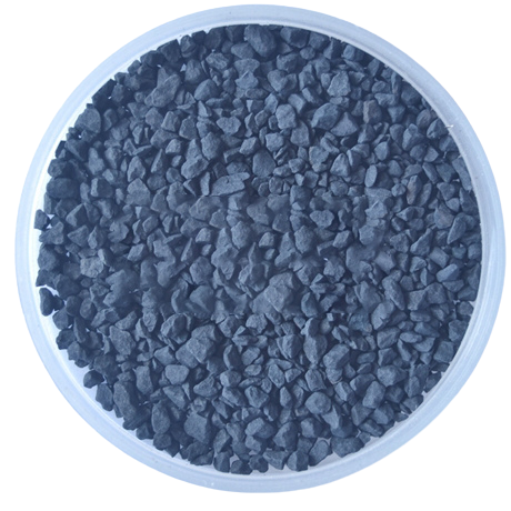
Gallium Arsenide particles are a kind of compound semiconductor particles mainly composed of Gallium and Arsenic, in the form of dark gray crystals or gray powder with metallic luster, with high density, high melting point, good electrical properties and certain chemical stability, which are widely used in semiconductors and photovoltaic and many other fields.
Characteristics
Chemical formula: GaAs
Appearance: usually dark gray crystals or gray powder, metallic luster, garlic smell when wet.
Density: Relatively high mass density, about 5.307g/cm³.
Melting point: melting point is 1238℃, decomposition starts at about 800℃ in vacuum, and the decomposition pressure of arsenic under the melting point is about 90kPa.
Thermal properties: coefficient of thermal expansion is 5.9×10-⁶, thermal conductivity 0.52W/(m・K), specific heat 0.086cal/g/°C, with good resistance to high temperature and radiation.
Electrical properties: belongs to the Ⅲ – V group compound semiconductor, with a direct bandgap structure, high electron mobility (about 8500cm ² / (v s)), high saturation drift speed and the effective mass of the electron is small and so on. This gives it good performance in high-frequency, high-speed electronic devices, such as those used in the manufacture of microwave and millimeter-wave devices such as RF power amplifiers and satellite communication equipment.
Stability: stable to oxygen and water vapor at room temperature, but arsenic vapor can be released when the temperature is above 480℃.
Solubility: insoluble in hydrochloric acid and water, slightly soluble in phosphate buffer (pH7.4) with a concentration of 0.1mol/L, soluble in nitric acid and aqua regia. Arsenic gas will be generated when reacting with strong reducing acid.
Applications
Semiconductor field:
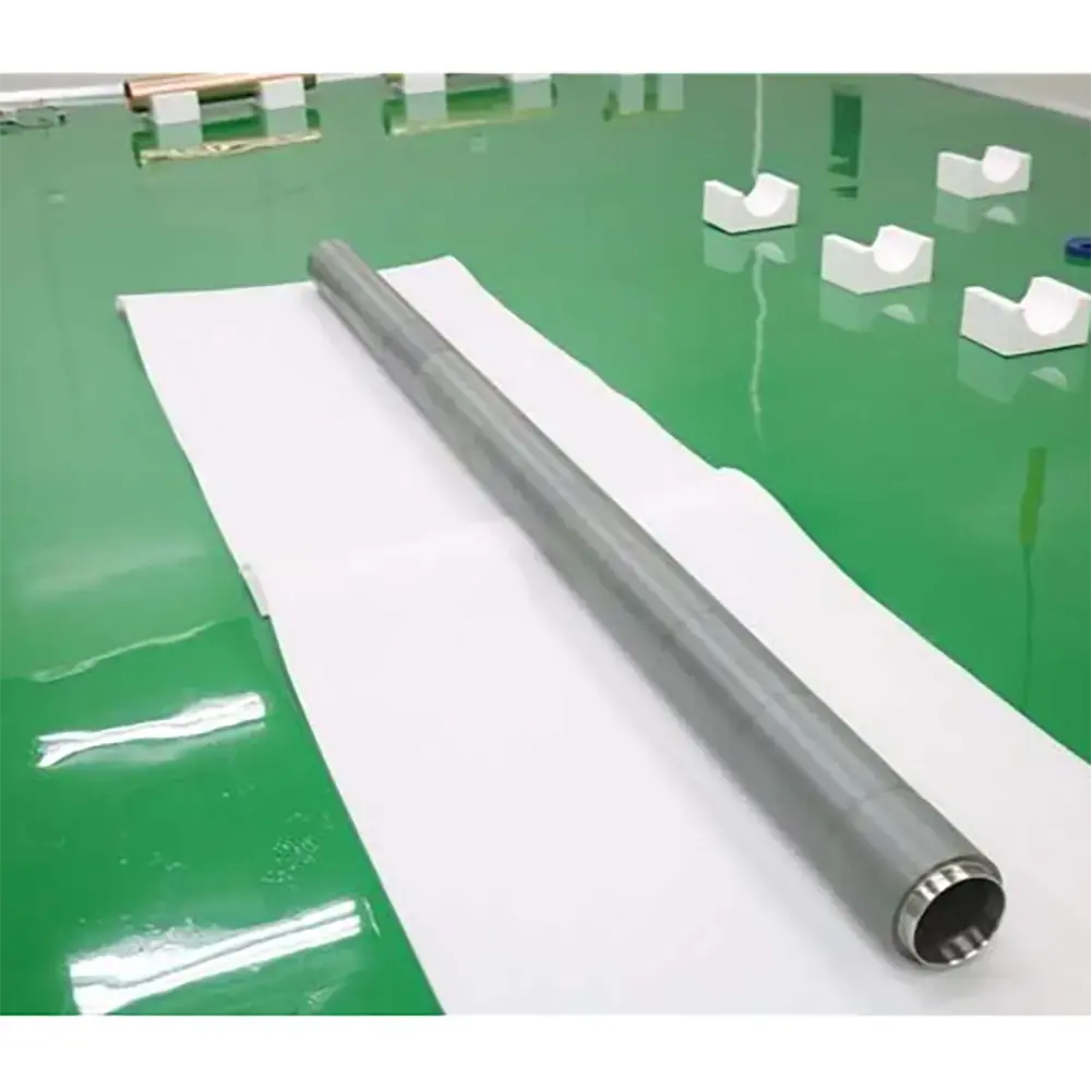
Integrated circuit manufacturing: Gallium Arsenide is an ideal semiconductor material in the manufacture of ultra-high-speed, high-frequency, low-noise integrated circuit chips. For example, it is used in the manufacture of high electron mobility transistors (HEMT), heterojunction bipolar transistors (HBT) and so on, and these devices are widely used in high-frequency fields such as wireless communications and satellite communications. Through sputtering target deposition technology, Gallium Arsenide films can be precisely formed on the wafer surface to provide high-performance semiconductor layers for integrated circuits.
Semiconductor laser manufacturing: GaAs sputtering targets can be used to manufacture the active layer of semiconductor lasers, which have important applications in the fields of optical communications, laser printing, laser medicine and other fields. The direct bandgap structure of Gallium Arsenide allows it to emit laser light efficiently, and the wavelength and performance of the laser light can be controlled by adjusting the composition and structure of the material.
Photovoltaic field:
Solar Cells: Gallium arsenide is an important photovoltaic material in thin film solar cells. Thin-film solar cells prepared using gallium arsenide sputtering targets have high photoelectric conversion efficiency and good stability, especially suitable for space applications and ground-based photovoltaic power stations with high efficiency requirements.
Light Emitting Diode (LED): GaAs-based LEDs have the advantages of high efficiency, high brightness, high color purity, etc. They can be used in indoor and outdoor lighting, display backlighting, automotive lighting and other fields. Through sputtering target technology, high quality GaAs film can be deposited on the LED chip to improve the luminous performance of LED.
Photodetector: GaAs photodetector has high sensitivity and response speed to infrared light, which can be used in infrared imaging, fiber optic communication, environmental monitoring and other fields. GaAs film prepared by sputtering target can improve the performance and stability of photodetectors.
Military and aerospace field:
Radar system: Gallium Arsenide sputtering targets can be used to manufacture microwave devices in radar systems, such as power amplifiers and low noise amplifiers. These devices are able to work at high frequency, characterized by high power output and low noise figure, which can improve the detection distance and resolution of radar.
Satellite communication: Satellite communication system needs high performance semiconductor devices to ensure the signal transmission quality and stability. Semiconductor devices made of GaAs sputtering target can work stably in the space environment and are suitable for transceivers, amplifiers and other components in satellite communications.
Other fields:
Biomedical field: gallium arsenide materials also have certain application prospects in the biomedical field, such as for the manufacture of biosensors, photothermal therapy equipment. Sputtering target technology can provide high-quality GaAs films for these applications.
Scientific research field: In the field of materials science, physics and other scientific research, GaAs sputtering target is an important tool to study the performance of semiconductor materials and prepare new semiconductor devices. Researchers can prepare GaAs films with different structures and properties through sputtering target technology to explore their physical properties and application potential under various conditions.
VI HALBLEITERMATERIAL GmbH (VIMATERIAL) employs a stringent quality assurance system to ensure the reliability of our product quality. Strict quality control is implemented throughout the entire production chain, and for defective products, we strictly enforce the principle of rework and redo. Each batch is released only after passing detailed specification tests.
Every batch of our materials is independently tested, and, if necessary, we send samples to certified companies for testing. We provide these documents and analysis certificates with the shipment to certify that our products meet the required standards.
Contact our team of experts today and let us help you with your business!