| Product ID | Formula | Purity | Dimension | Quantity | Price in € | Inquiry |
|---|---|---|---|---|---|---|
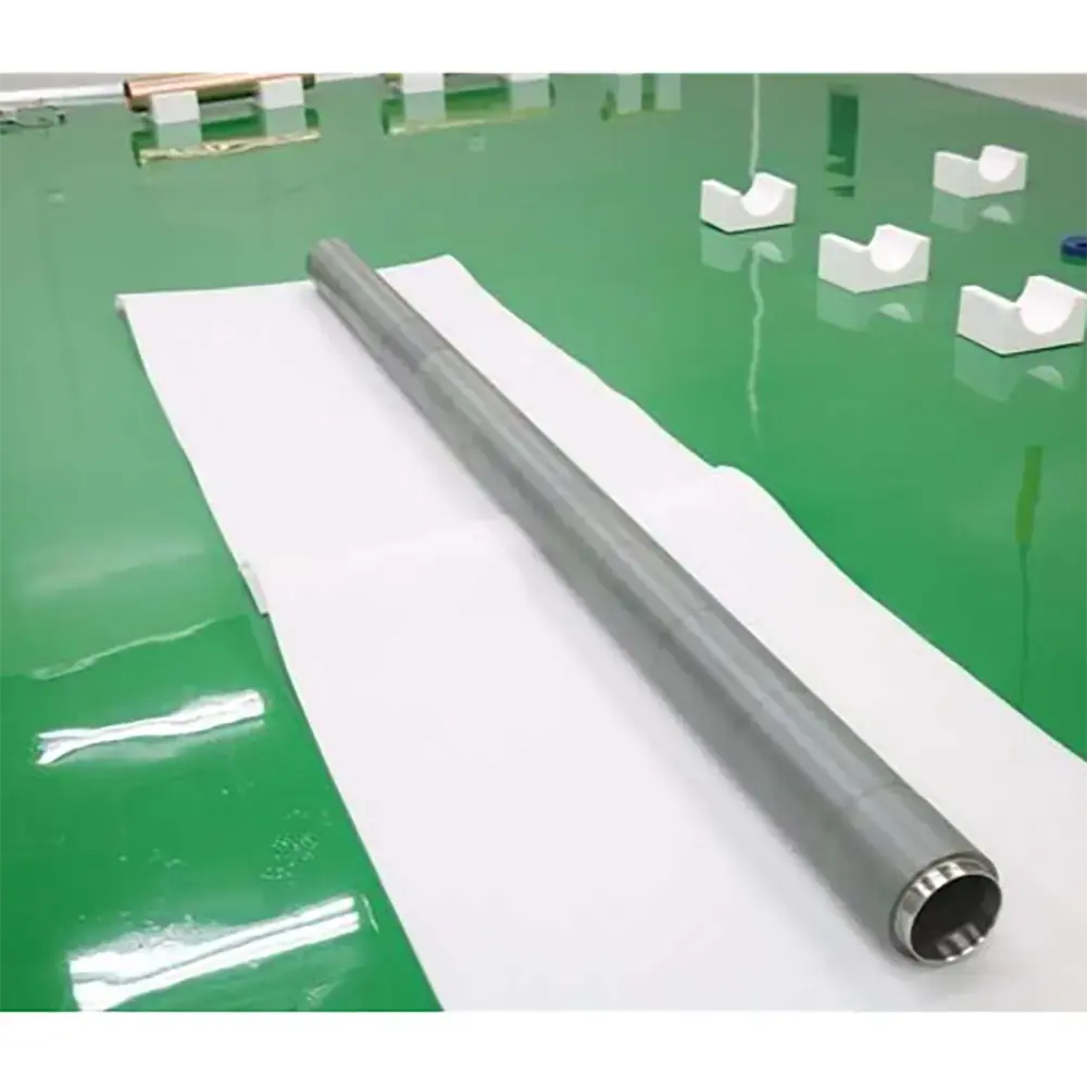
| 293401ST001 | CuSe | 99.99% | Ø 50.8 mm x 6.35 mm | 1 | POR | Inquire |
| 293401ST002 | CuSe | 99.99% | Ø 76.2 mm x 6.35 mm | 1 | POR | Inquire |
| 293401ST003 | CuSe | 99.99% | Ø 101.6 mm x 3.175 mm | 1 | POR | Inquire |
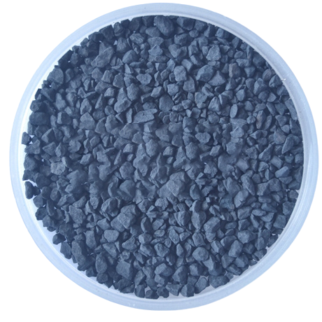
Copper Selenide sputtering target is a material composed of copper and selenium used in magnetron sputtering and other coating processes to prepare thin films with specific properties, which have important applications in semiconductor, photovoltaic and other fields.
VIMATERIAL provides high purity Copper Selenide sputtering targets, we are a professional supplier of inorganic chemical raw materials, our targets are characterized by high purity, good surface flatness, stable product performance and good product consistency. We support customized service and binding service, if you have technical problems, please contact us.
Molecular formula: CuSe
Molecular weight: 142.5
Appearance: blue-black color
Density: 5.99 g/mL (25℃)
Melting point: 550°C
Photovoltaic field: Widely used in the manufacture of solar cells, the thin film deposited on the substrate through sputtering technology can be used as an absorbing layer material, effectively absorbing sunlight, improve photoelectric conversion efficiency, and help the development of solar photovoltaic power generation technology.
Semiconductor field: In the process of semiconductor device production, the sputtering target can deposit a thin film with specific electrical properties, which is used to manufacture part of the functional layer of the semiconductor chip, such as the formation of p-n junction, to provide a suitable channel for the conduction and control of electrons, and to improve the performance of semiconductor devices.
Optoelectronics: Used as a key layer in the preparation of optoelectronic devices such as photodetectors and light-emitting diodes, deposited Copper Selenide films optimize the absorption, emission, and conversion of light in optoelectronic devices, for example, by improving the sensitivity of photodetectors to specific wavelengths of light.
Electronics: In the manufacture of electronic devices, thin films deposited by this sputtering target can improve the contact and electrical properties of electronic components, and can be used as electrode or connecting materials to enhance the efficiency and stability of current transfer within electronic devices.
Each batch of products has a strict quality system to ensure that the complete inspection records, all ex-factory products can be traced, and will provide samples to the customer after the factory, for customers to re-inspection. We have good product consistency and high product reproducibility.
Copper Selenide sputtering targets are generally protected by double vacuum bagging followed by box packing.
Copper Selenide sputtering targets should be stored in a dry, cool, well-ventilated and light-proof environment, sealed to prevent moisture and oxidation, avoid mechanical collision of the target, and at the same time keep it away from ignition sources, heat sources and chemically active substances to ensure the performance and quality of the target.
VI HALBLEITERMATERIAL GmbH (VIMATERIAL) employs a stringent quality assurance system to ensure the reliability of our product quality. Strict quality control is implemented throughout the entire production chain, and for defective products, we strictly enforce the principle of rework and redo. Each batch is released only after passing detailed specification tests.
Every batch of our materials is independently tested, and, if necessary, we send samples to certified companies for testing. We provide these documents and analysis certificates with the shipment to certify that our products meet the required standards.
Contact our team of experts today and let us help you with your business!