| Product ID | Formula | Purity | Dimension | Quantity | Price in € | Inquiry |
|---|---|---|---|---|---|---|
| 2949313400ST001 | CuInGaSe | 99.99% | Ø 25.4 mm x 3.175 mm | 1 | POR | Inquire |
| 2949313400ST002 | CuInGaSe | 99.99% | Ø 50.8 mm x 3.175 mm | 1 | POR | Inquire |
| 2949313400ST003 | CuInGaSe | 99.99% | Ø 50.8 mm x 6.35 mm | 1 | POR | Inquire |
| 2949313400ST004 | CuInGaSe | 99.99% | Ø 76.2 mm x 6.35 mm | 1 | POR | Inquire |
| 2949313400ST005 | CuInGaSe | 99.99% | Ø 152.4 mm x 6.35 mm | 1 | POR | Inquire |
| 2949313400ST006 | CuInGaSe | 99.99% | Ø 203.2 mm x 6.35 mm | 1 | POR | Inquire |
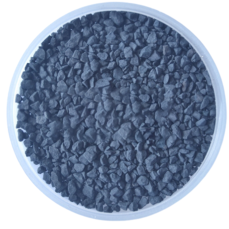
Copper Indium Gallium Selenide sputtering target is a key material for magnetron sputtering coating technology with high purity and specific composition ratio, which has important applications in photovoltaic cells, electronic devices and other fields.
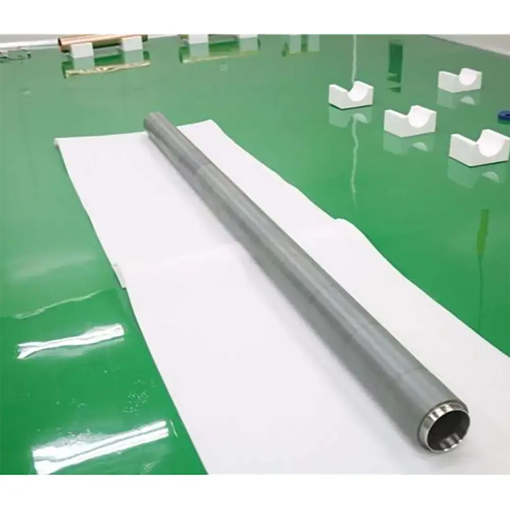
VImaterial is able to provide high purity and high quality Copper Indium Gallium Selenide sputtering targets with customised ratios for production by our dedicated technical team. Our targets have excellent surface flatness and finish and we can also provide a binding service. If you have any questions, please feel free to contact us.
Molecular formula: CuInGaSe
Appearance: Usually grey target, surface has a certain metallic luster, relatively brittle texture .
Density: about 5.7-5.9g/cm3
Crystal structure: belongs to the tetragonal crystal system, with a structure similar to chalcopyrite.
Photovoltaic field: used in the preparation of copper indium gallium selenide thin film solar cell absorber layer, can improve the photoelectric conversion efficiency of the cell.
Semiconductor field: In the manufacture of integrated circuits, it can be used to make high-performance interconnect and contact electrodes to ensure the efficient and stable operation of circuits.
Display field: In the production of thin-film transistors for liquid crystal displays and organic light-emitting diode (OLED) displays, it is used to produce high-performance semiconductor layers to ensure the reliable operation of the display.
Optoelectronic device field: can be used in the manufacture of light-emitting diodes and laser diodes and other optoelectronic devices, to enhance the performance of the device.
R&D of energy batteries, which helps to improve the energy density and charging/discharging performance of batteries.
Each batch of products will be inspected, our production process has a strict quality control system, from raw materials to the final inspection, each production link has self-inspection and re-inspection, and IPQC inspection. We also provide samples for customers to re-inspection, if the customer has a designated inspection organisation, we also support third party inspection and issue inspection reports.
Copper Indium Gallium Selenide sputtering targets are usually packed in double vacuum bags.
Copper Indium Gallium Selenide sputtering targets should be stored in a dry, cool, well-ventilated environment protected from light, in sealed packages to prevent moisture and oxidation, while avoiding contact with corrosive substances such as acids and alkalis, and away from high temperatures and possible mechanical collision, in order to maintain the integrity and chemical stability of the target.
VI HALBLEITERMATERIAL GmbH (VIMATERIAL) employs a stringent quality assurance system to ensure the reliability of our product quality. Strict quality control is implemented throughout the entire production chain, and for defective products, we strictly enforce the principle of rework and redo. Each batch is released only after passing detailed specification tests.
Every batch of our materials is independently tested, and, if necessary, we send samples to certified companies for testing. We provide these documents and analysis certificates with the shipment to certify that our products meet the required standards.
Contact our team of experts today and let us help you with your business!