| Product ID | Formula | Purity | Dimension | Quantity | Price in € | Inquiry |
|---|---|---|---|---|---|---|
| 29493100ST001 | CuInGa | 99.99% | Ø 76.2 mm x 6.35 mm | 1 | POR | Inquire |
| 29493100ST002 | CuInGa | 99.99% | Ø 152.4 mm x 6.35 mm | 1 | POR | Inquire |
| 29493100ST003 | CuInGa | 99.99% | Ø 203.2 mm x 6.35 mm | 1 | POR | Inquire |
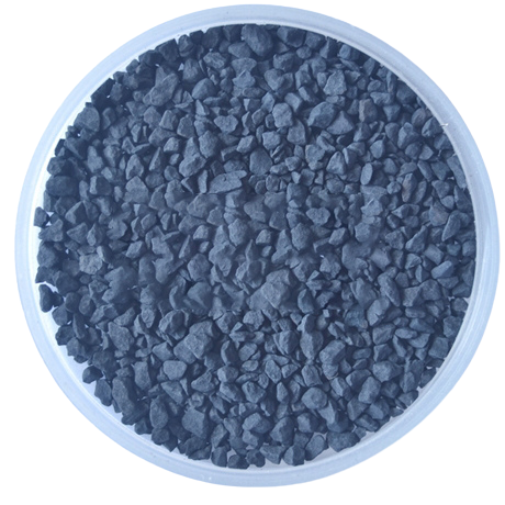
Copper Indium Gallium sputtering target is a key basic material composed of copper, indium, gallium and other elements used for the preparation of thin film materials by sputtering process, which has important applications in the fields of electronics and semiconductors.
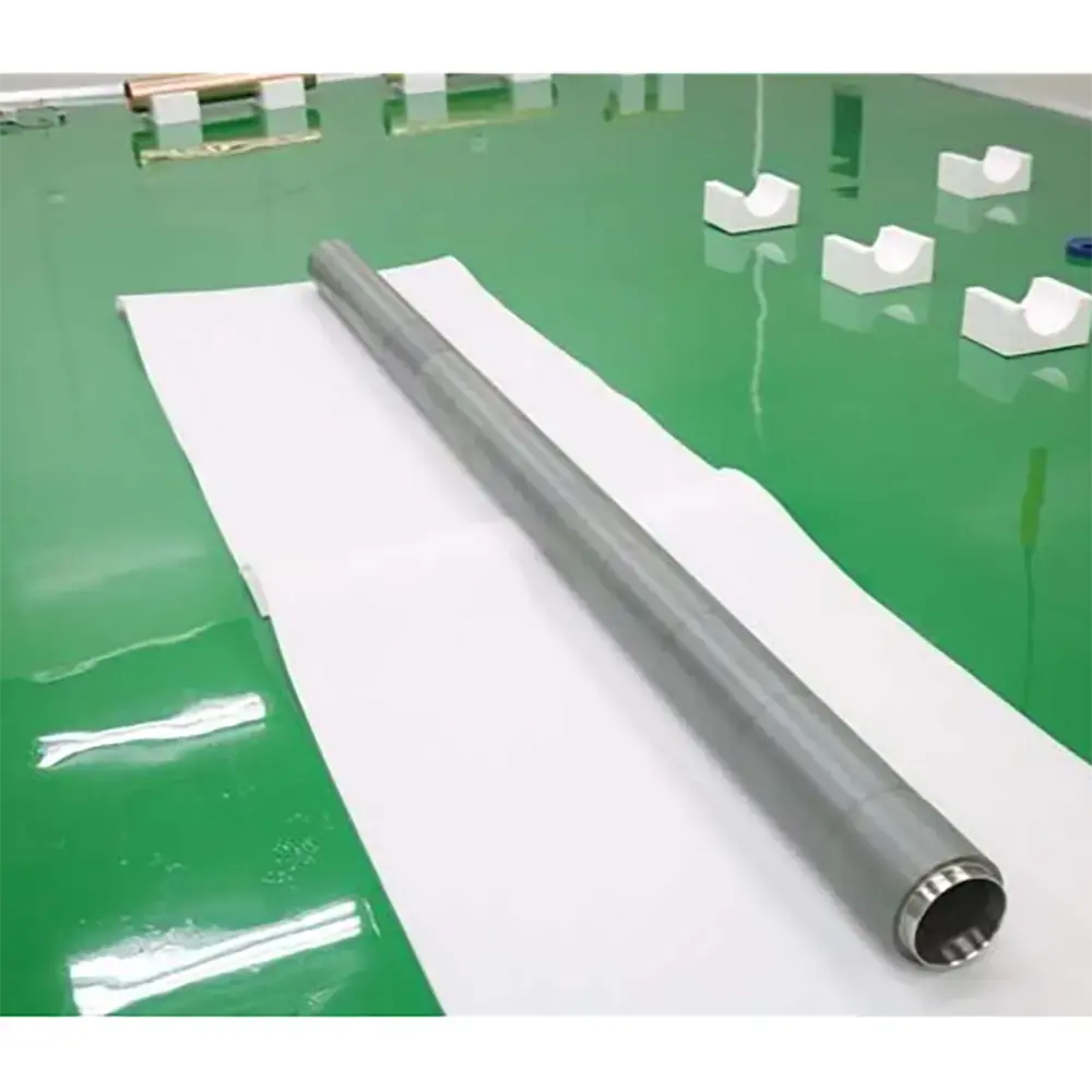
VImaterial offers high-purity and high-quality Copper Indium Gallium sputtering targets with excellent surface finish, flatness and stability. We also offer customized sizes and ratios, as well as target binding services, so please contact us soon.
Molecular formula: CuInGa
Appearance: usually black or gray-black solid
Density: The density of CIGS is about 5.7-5.9g/cm3.
Melting point: CIGS is a polymer compound, about 1050-1100°C
Crystal structure: CIGS has a chalcopyrite structure and belongs to the tetragonal crystal system.
Solar photovoltaic field: used in the production of copper indium gallium selenide (CIGS) thin-film solar cells, which have the advantages of high efficiency, flexibility, etc., and can be used in a variety of scenarios, such as building-integrated photovoltaic.
Semiconductor field: Used as a key material in the thin film deposition of chips and other electronic devices, which helps to improve device performance and integration.
Optical communication field: It plays an important role in the manufacture of optical communication devices, and can be used to deposit relevant thin films to improve optical performance and communication efficiency.
Aerospace field: It can be used to manufacture high-performance electronic components and optical parts in aerospace equipment to meet the stringent requirements for material performance and reliability.
Automotive field: applied to the production of automotive electronic components, such as sensors, displays, etc., to enhance the level of automotive intelligence and information technology.
Each batch of products need to check the size and composition, we can also provide samples for customers to re-inspection. If you need a third party inspection organization to inspect, we also support.
Copper Indium Gallium sputtering targets are generally packed in double vacuum bags, or can be boxed for protection.
Copper Indium Gallium sputtering targets should be stored in vacuum packaging with a built-in moisture barrier to avoid moisture, oxidation and exposure to impurities.
VI HALBLEITERMATERIAL GmbH (VIMATERIAL) employs a stringent quality assurance system to ensure the reliability of our product quality. Strict quality control is implemented throughout the entire production chain, and for defective products, we strictly enforce the principle of rework and redo. Each batch is released only after passing detailed specification tests.
Every batch of our materials is independently tested, and, if necessary, we send samples to certified companies for testing. We provide these documents and analysis certificates with the shipment to certify that our products meet the required standards.
Contact our team of experts today and let us help you with your business!