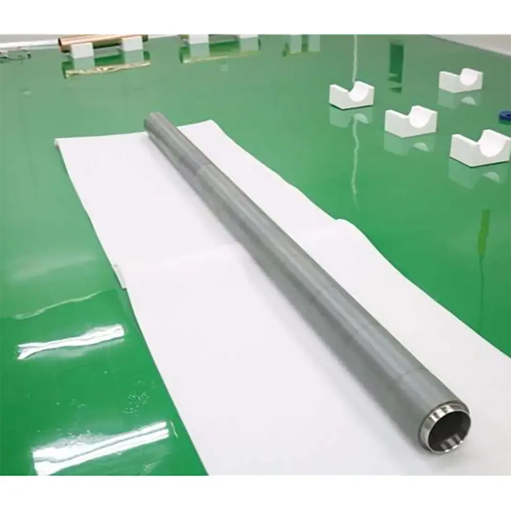
Cesium Iodide sputtering target is a material used in sputtering deposition technology. With cesium iodide as the main component, its surface atoms detach and deposit on the substrate to form a thin film after being bombarded by an ion beam in a high-vacuum environment, which is widely used as a key functional material in semiconductors, optics, medical treatment and other fields.
Characteristics
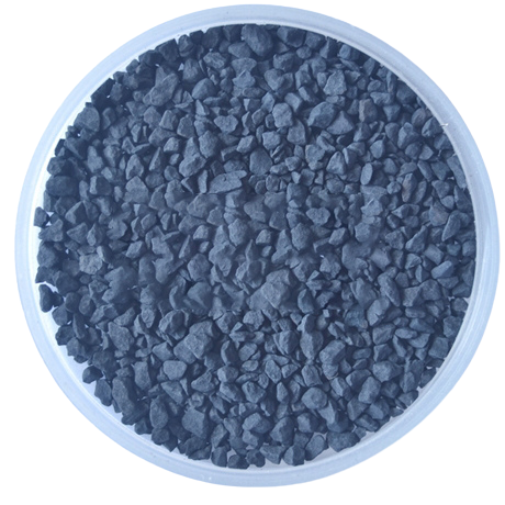
Appearance: usually white crystalline solid
Crystal structure: Cubic crystal structure, this crystal structure makes the atomic arrangement in the sputtering process has a certain direction and regularity, which helps to form high-quality thin films.
Density: about 4.5 g/cm³, the relatively high density enables it to maintain good stability during the sputtering process, reducing the pores and defects inside the target material, thus improving the quality of sputtered films.
Melting point: 620°C (1150°F), the high melting point ensures that the target can withstand high energy bombardment during the sputtering process without melting and deformation, ensuring the stability of the sputtering process and the service life of the target.
Boiling point: 1277°C (2331°F), the higher boiling point makes the target less likely to evaporate rapidly due to high temperature during sputtering, which is conducive to controlling the sputtering rate and film growth process.
Thermal Conductivity: At 298K (i.e. 25°C), the thermal conductivity is about 1.1 W/m K. The low thermal conductivity means that the target can retain heat well during the sputtering process, which makes the temperature in the sputtering area relatively stable and is conducive to the improvement of the uniformity of the sputtered film.
Coefficient of thermal expansion: about 48 µm/m・K. The coefficient of thermal expansion affects the dimensional stability of the target material when the temperature changes, and this value indicates that the cesium iodide sputtering target material will expand to a certain extent when the temperature changes, but the degree of expansion is relatively within the acceptable range.
Refractive index: about 1.9, the high refractive index gives it certain advantages in optical applications, for example, in the preparation of optical films to produce better refraction and reflection of light.
Hardness: Moderate hardness to ensure that it is not easily damaged during sputtering, but also easy to process and manufacture.
Solubility: soluble in water and alcohols. It is easily oxidised by oxygen in humid air, so attention needs to be paid to moisture-proofing and anti-oxidation during storage and use.
Chemical reactivity: Cesium iodide can react with silver nitrate to generate silver iodide precipitate; it can react with iodine to generate stable cesium triiodide; it can also be oxidised by strong oxidising agents such as sodium hypochlorite, sodium bismuthate, nitric acid, permanganic acid and chlorine gas.
Application
Semiconductor field:
Thin film deposition: used to deposit thin films in the semiconductor manufacturing process. Cesium iodide targets form thin films on the surface of semiconductor chips by sputtering process, and these films can be used as insulating layers, conductive layers or other functional layers of semiconductor devices, which play an important role in the performance and reliability of semiconductor devices. For example, in some special semiconductor device structures, cesium iodide films can provide specific electrical or optical properties.
Doping source: It can be used as a source of dopant materials. The caesium or iodine element in caesium iodide is doped into the semiconductor material through sputtering to change the electrical properties of the semiconductor, such as adjusting its conductive type (N-type or P-type) and carrier concentration, etc., to meet the needs of different semiconductor devices.
Optical field:
Optical coatings: used to prepare optical thin film coatings, such as transmittance enhancement film, reflective film, etc. Cesium iodide sputtering targets can deposit thin films with specific optical properties on the surface of optical elements to improve the transmittance, reflectivity or anti-reflective properties of the optical elements. For example, in optical lenses, lasers, solar cells and other optical devices, cesium iodide films can reduce the reflection and scattering of light and improve the optical efficiency of the device.
Infrared detectors: In the manufacture of infrared detectors, cesium iodide thin films can be used as sensitive materials for detectors with high absorption and response to infrared radiation, which can improve the sensitivity and detection performance of infrared detectors.
Medical imaging field:
X-ray detector: Cesium iodide is a commonly used X-ray detector material. X-ray detectors prepared with cesium iodide sputtering targets have high detection efficiency and sensitivity, and can quickly and accurately detect the intensity and energy distribution of X-rays, which are widely used in medical X-ray imaging, industrial non-destructive testing and other fields. For example, in medical X-ray machines, CT scanners and other equipment, cesium iodide detectors can convert X-rays into electrical signals, generating high-quality medical images to help doctors diagnose and treat diseases.
Nuclear medicine imaging: In nuclear medicine imaging equipment, such as positron emission tomography (PET) and single photon emission computed tomography (SPECT), cesium iodide film can be used as the scintillator material of the detector, which converts gamma rays emitted by radionuclides into visible light, and then converts the visible light into electrical signals through photodetectors to realise the imaging of the radioactive distribution inside the human body.
Flat panel display field:
Liquid Crystal Display (LCD): In the LCD manufacturing process, cesium iodide sputtering targets are used to prepare electrode materials or other functional films in liquid crystal panels. These films can improve the electrical properties, optical properties and stability of liquid crystal displays, and improve display effects, such as increasing contrast, response speed and colour saturation.
Organic light-emitting diode (OLED) displays: Although OLED displays mainly use organic materials to emit light, cesium iodide films can also play a role in some auxiliary structures or functional layers, such as as encapsulation layers or electrode modification layers, to improve the performance and life of OLED displays.
VI HALBLEITERMATERIAL GmbH (VIMATERIAL) employs a stringent quality assurance system to ensure the reliability of our product quality. Strict quality control is implemented throughout the entire production chain, and for defective products, we strictly enforce the principle of rework and redo. Each batch is released only after passing detailed specification tests.
Every batch of our materials is independently tested, and, if necessary, we send samples to certified companies for testing. We provide these documents and analysis certificates with the shipment to certify that our products meet the required standards.
Contact our team of experts today and let us help you with your business!