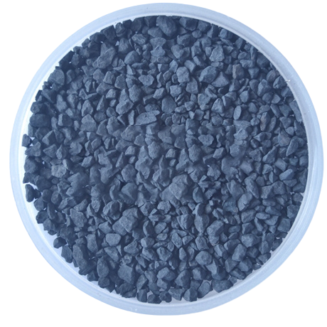
Cadmium Oxide sputtering target is a kind of key material used in sputtering coating process, with cadmium oxide as the main component, cadmium oxide material can be deposited onto the substrate to form a thin film, which is widely used in the field of electronics, optics, semiconductors and so on, and has a higher purity and specific physical morphology to meet the requirements of the sputtering process.
Characteristics
Chemical formula: CdO
Molecular weight: 128.4
Colour and appearance: red
Density: 8.15 g/cm³
Melting point: 900 – 1000 °C (1652 – 1832 °F)
Boiling point: 1559 °C (2838 °F)
Applications
Solar cell field:
In the manufacture of thin film solar cells, it can be used to prepare functional films for solar cells. Using sputtering technology to deposit cadmium oxide on a substrate to form a thin film can improve the photoelectric conversion efficiency and performance stability of solar cells. Compared with the traditional silicon-based solar cells, the use of cadmium oxide sputtering target preparation of thin film solar cells can greatly reduce the amount of material, reduce manufacturing costs, and has the advantages of low manufacturing temperature, wide range of applications.
Flat panel display field:
In liquid crystal display (LCD), organic light-emitting diode (OLED) and other flat panel display technology, can be used to prepare transparent conductive films or other functional films. These films have an important impact on the performance of flat panel displays, such as conductivity, light transmission, colour display and so on.
Optical coating field:
It is used to manufacture optical lenses, filters, mirrors and other optical components for coating. Cadmium oxide films have specific optical properties, such as good transmittance or reflectivity for specific wavelengths of light. Cadmium oxide deposited on the surface of optical components through the sputtering coating process can achieve precise regulation of optical properties to meet the needs of different optical applications, such as lasers, optical sensors, optical communications and other fields of optical components in the manufacture of important applications.
Semiconductor field:
In the manufacturing process of semiconductor devices, it can be used to prepare semiconductor thin films, such as in the metallisation process of semiconductor chips, for the formation of insulating layers or gate materials in metal oxide semiconductor (MOS) structures. Although the semiconductor field has very high requirements for the purity and quality of the target material, cadmium oxide has a unique application value in some specific semiconductor processes to improve the performance and reliability of semiconductor devices.