


Silicon is best known as the foundation of semiconductor chips and solar cells. However, one of its most important high-value applications is often overlooked: silicon sputtering targets. As a critical material for physical vapor deposition (PVD), silicon targets play an essential role in manufacturing semiconductors, flat panel displays, photovoltaic devices, and advanced optical coatings.
Although rarely seen by end users, silicon sputtering targets are indispensable to modern electronics. They directly influence thin film quality, device performance, and manufacturing reliability.
What Is a Silicon Sputtering Target?
A silicon sputtering target is a high-purity silicon material manufactured into a disc, plate, or tube for use in magnetron sputtering, one of the most widely used Physical Vapor Deposition (PVD) technologies.
During the sputtering process, energetic ions bombard the silicon target inside a vacuum chamber, ejecting silicon atoms from its surface. These atoms travel through the vacuum and deposit onto substrates such as semiconductor wafers, glass, ceramics, or metals, forming an extremely thin and uniform silicon film.
Because thin-film properties largely depend on the quality of the target material, silicon sputtering targets are considered one of the key consumables in advanced thin-film manufacturing.
Types of Silicon Sputtering Targets
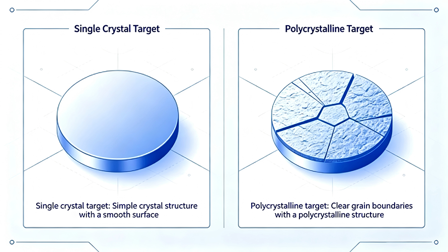
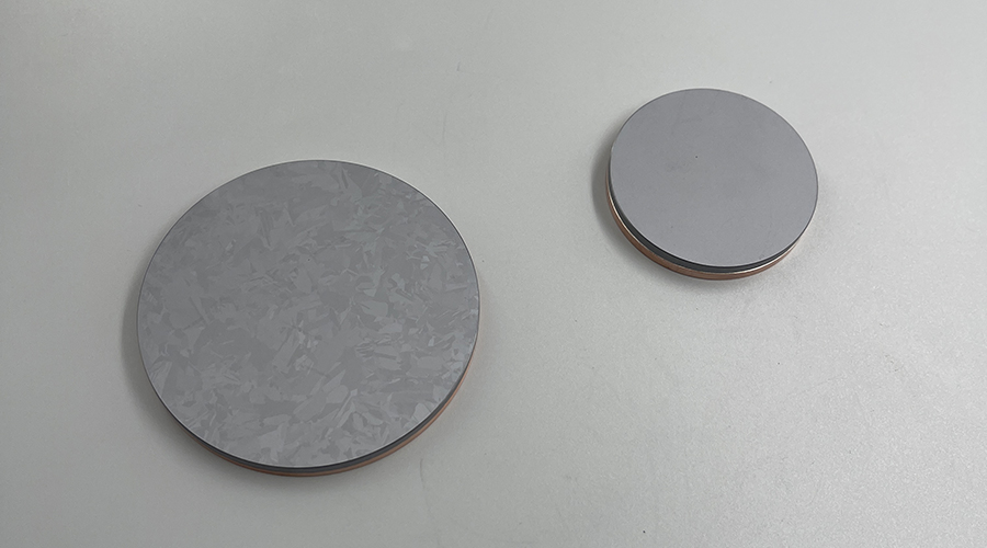
Silicon sputtering targets are generally classified into single-crystal and polycrystalline types. Although both are used for thin-film deposition, they differ in crystal structure, purity, manufacturing cost, and typical applications.
Single Crystal vs. Polycrystalline Silicon Targets
| Feature | Single-Crystal Silicon Target | Polycrystalline Silicon Target |
|---|---|---|
| Crystal Structure | Continuous single crystal lattice | Multiple silicon grains |
| Typical Purity | 6N (99.9999%) or higher | 4N–5N (99.99%–99.999%) |
| Uniformity | Excellent | Very good |
| Manufacturing Cost | Higher | Lower |
| Sputtering Stability | Excellent | Excellent |
| Main Applications | Semiconductor manufacturing | Solar cells, flat panel displays, optical coatings |
| Typical Users | Chip manufacturers | Photovoltaic, display and coating industries |
Single-Crystal Silicon Target
Single-crystal silicon targets feature a continuous crystal lattice without grain boundaries. They typically offer purity levels of 99.9999% (6N) or higher, providing exceptional structural uniformity and minimal impurities.
Their superior crystal quality makes them ideal for demanding semiconductor applications where film uniformity and electrical performance are critical. However, manufacturing single-crystal targets is technically challenging and relatively expensive.
Polycrystalline Silicon Target
Polycrystalline silicon targets consist of numerous fine silicon grains consolidated through advanced manufacturing processes. They generally provide purity levels ranging from 99.99% (4N) to 99.999% (5N) while offering excellent sputtering stability and lower production costs.
Because of their balance between performance and cost, polycrystalline silicon targets are widely used in large-scale industrial coating applications.
Typical Specifications of Silicon Sputtering Targets
Silicon sputtering targets can be manufactured in a variety of purity grades, crystal structures, and dimensions to meet different deposition requirements. The following table summarizes the most common specifications available for industrial and research applications.
| Parameter | Typical Value |
|---|---|
| Material | Silicon (Si) |
| Purity | 99.99%–99.9999% |
| Crystal Type | Single Crystal / Polycrystalline |
| Density | ≥99% of theoretical density |
| Shape | Round, Rectangular, Rotary |
| Backing Plate | Optional (Copper, CuCr, Molybdenum, Stainless Steel) |
| Manufacturing Method | Precision machining |
| Compatible Deposition Methods | DC, RF and Pulsed DC Magnetron Sputtering |
The exact specifications should be selected based on the deposition process, coating material, equipment configuration, and performance requirements. Many manufacturers also provide customized dimensions, bonding options, and purity grades to meet specific industrial or research needs.
How Does a Silicon Sputtering Target Work?
The operating principle of a silicon sputtering target is based on magnetron sputtering, a highly efficient PVD process.
The basic process consists of the following steps:
- A silicon target is mounted onto the cathode inside a vacuum deposition chamber.
- Argon gas is introduced into the chamber and ionized into plasma.
- Positively charged argon ions accelerate toward the negatively charged silicon target.
- The high-energy ion bombardment ejects silicon atoms from the target surface.
- These silicon atoms travel through the vacuum and condense onto the substrate, forming a dense and uniform thin film.
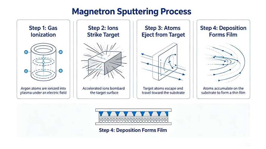
This process enables precise control of film thickness, composition, and microstructure, making it indispensable for advanced electronics manufacturing.
Key Properties of Silicon Sputtering Targets
The performance of a sputtering target directly affects coating quality. High-quality silicon targets typically exhibit the following characteristics:
Ultra-High Purity
Purity is the most critical parameter. Semiconductor-grade silicon targets generally require purity levels of 5N (99.999%) or higher, while leading-edge semiconductor processes often require 6N (99.9999%) silicon to minimize contamination.
High Density
A dense, pore-free structure reduces particle generation during sputtering and improves coating uniformity.
Uniform Microstructure
Consistent grain size and homogeneous internal structure help maintain stable sputtering rates and produce films with excellent thickness uniformity.
Excellent Thermal Conductivity
Good thermal conductivity improves heat dissipation during sputtering, reducing thermal stress and extending target service life.
Applications of Silicon Sputtering Targets
Silicon sputtering targets are widely used across numerous high-tech industries.
Semiconductor Manufacturing
Silicon targets are used to deposit polysilicon films, insulating layers, and functional thin films in integrated circuit fabrication. Film quality directly influences device performance, reliability, and production yield.
Photovoltaic Industry
Silicon thin films produced by sputtering are used in thin-film solar cells, passivation layers, and photovoltaic device fabrication, contributing to improved photoelectric conversion efficiency.
Flat Panel Displays
LCD and OLED display manufacturing relies on silicon-based thin films for thin-film transistors (TFTs), enabling high-resolution displays and precise touch functionality.
Optical Coatings
Silicon sputtering targets are widely used to manufacture optical films for infrared optics, anti-reflection coatings, beam splitters, filters, and precision optical components.
Consumer Electronics
Silicon thin films provide functional coatings for smartphones, wearable devices, camera modules, and protective glass, improving optical performance, electrical properties, and durability.
| Industry | Thin Film Produced | Typical Applications |
|---|---|---|
| Semiconductor | Silicon thin films | Integrated circuits (ICs), MEMS devices |
| Solar Energy | Amorphous and microcrystalline silicon films | Thin-film photovoltaic cells |
| Flat Panel Displays | TFT silicon films | LCD and OLED displays |
| Optics | Optical silicon coatings | Infrared optics, anti-reflection coatings, filters |
| Consumer Electronics | Functional silicon coatings | Smartphones, wearable devices, camera modules |
Why Silicon Sputtering Targets Matter?
Producing a high-quality silicon sputtering target requires advanced purification technologies, precision machining, crystal structure control, bonding techniques, and rigorous quality inspection.
Even trace amounts of impurities or structural defects can lead to particle generation, unstable sputtering, poor film quality, or device failure. As semiconductor nodes continue to shrink and electronic devices become increasingly sophisticated, manufacturers demand silicon targets with higher purity, tighter tolerances, and more consistent performance than ever before.
How to Select the Right Silicon Sputtering Target?
Choosing the right silicon sputtering target depends on the deposition process and application requirements. The most important factors include purity, crystal structure, target dimensions, and bonding configuration.
| Selection Factor | Recommendation |
|---|---|
| Purity | 5N for general electronics; 6N or higher for semiconductor manufacturing. |
| Crystal Structure | Single crystal for precision devices; polycrystalline for industrial coating. |
| Target Shape | Select round, rectangular, or rotary targets according to the sputtering system. |
| Backing Plate | Use bonded targets for improved cooling and high-power sputtering. |
| Deposition Method | Ensure compatibility with DC, RF, or pulsed DC magnetron sputtering. |
| Application | Match target specifications to semiconductor, photovoltaic, optical, or display requirements. |
Selecting the appropriate specifications helps achieve stable deposition, high-quality thin films, and longer target service life.
Conclusion
Although largely invisible to consumers, silicon sputtering targets are among the most important enabling materials in modern technology. From semiconductor chips and solar panels to display panels, optical systems, and consumer electronics, they support the production of countless devices used every day.
As industries such as semiconductors, renewable energy, artificial intelligence, and advanced electronics continue to evolve, the demand for higher-performance silicon sputtering targets will only increase. Their importance as a foundational material for next-generation thin-film technologies will continue to grow, making silicon sputtering targets an essential component of the future of advanced manufacturing.
FAQs
What is a silicon sputtering target?
A silicon sputtering target is a high-purity silicon material used in Physical Vapor Deposition (PVD), particularly magnetron sputtering. During deposition, silicon atoms are sputtered from the target and deposited onto a substrate to form uniform thin films used in semiconductors, displays, solar cells, and optical devices.
What purity is required for a silicon sputtering target?
The required purity depends on the application.
- 4N (99.99%) – Suitable for general industrial coatings.
- 5N (99.999%) – Commonly used in photovoltaic and display industries.
- 6N (99.9999%) or higher – Required for advanced semiconductor manufacturing where extremely low impurity levels are critical.
Higher purity generally results in fewer contaminants, better film quality, and improved device performance.
What is the difference between single-crystal and polycrystalline silicon targets?
Single-crystal silicon targets have a continuous crystal structure with no grain boundaries, offering superior uniformity and purity. They are mainly used in high-end semiconductor manufacturing.
Polycrystalline silicon targets consist of multiple silicon grains and provide excellent sputtering stability at a lower cost, making them suitable for photovoltaics, flat panel displays, and optical coatings.
What are silicon sputtering targets used for?
Silicon sputtering targets are widely used in:
- Semiconductor integrated circuits (ICs)
- Thin-film solar cells
- LCD and OLED displays
- Optical coatings
- MEMS devices
- Infrared optics
- Protective and functional coatings
What shapes are silicon sputtering targets available in?
Silicon sputtering targets can be manufactured in various geometries, including:
- Round targets
- Rectangular targets
- Rotary (tube) targets
- Custom-shaped targets
The appropriate design depends on the sputtering system and coating application.
What factors affect the lifetime of a silicon sputtering target?
Target lifetime depends on several factors, including:
- Target purity
- Density
- Grain structure
- Cooling efficiency
- Sputtering power
- Process pressure
- Target utilization rate
Proper process optimization can significantly extend target service life.
How do I choose the right silicon sputtering target?
Selecting the appropriate silicon target depends on:
- Required purity
- Crystal structure (single crystal or polycrystalline)
- Target dimensions
- Deposition method
- Backing plate requirements
- Application industry
- Equipment compatibility
Working with an experienced sputtering target supplier helps ensure the target meets both equipment specifications and coating performance requirements.