


What Is an Indium Tin Oxide (ITO) Sputtering Target?
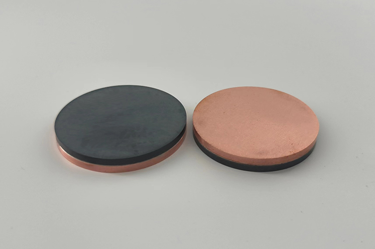
An Indium Tin Oxide (ITO) sputtering target is a transparent conductive oxide (TCO) material widely used for depositing transparent conductive films. The standard composition consists of 90 wt.% indium oxide (In₂O₃) and 10 wt.% tin oxide (SnO₂), a ratio carefully optimized to achieve an excellent balance between electrical conductivity and optical transparency.
Rather than being a simple mixture, ITO is a precisely engineered ceramic material. Indium oxide is an n-type semiconductor with a wide band gap of approximately 3.6 eV, allowing high visible-light transmission while providing good electrical conductivity through free electrons. Tin oxide acts as a dopant that increases the carrier concentration in indium oxide, significantly reducing electrical resistivity without sacrificing transparency.
The combination of In₂O₃ and SnO₂ also stabilizes the material by reducing conductivity fluctuations caused by oxygen vacancies. As a result, ITO films exhibit excellent electrical performance, high optical transmittance, and outstanding long-term stability.
Because of these properties, ITO remains one of the most widely used transparent conductive materials for applications such as:
- Flat-panel displays
- Touch screens
- OLED devices
- Solar cells
- Low-emissivity (Low-E) glass
- Smart windows
- Optical coatings
Common Problems and Solutions During ITO Thin Film Deposition
A. Film Peeling and Cracking
Film delamination and cracking are among the most common issues encountered during ITO thin-film deposition. These defects reduce conductivity, optical performance, and mechanical reliability, ultimately shortening the service life of coated components.
Causes
1. Residual Stress
Residual stress is generated because the thermal expansion coefficients of the ITO film and substrate are different. During high-temperature deposition and subsequent cooling, thermal stress accumulates inside the film. Excessive stress may lead to cracking or complete film delamination, particularly on flexible substrates.
2. Poor Substrate Preparation
Contaminants such as grease, dust, moisture, or native oxide layers reduce film adhesion. If the substrate surface is not properly cleaned or activated before deposition, the bonding strength between the substrate and the ITO coating decreases significantly.
3. Excessive Film Thickness
Depositing an excessively thick ITO layer in a single process increases internal stress. Thick films are also more susceptible to mechanical stress during bending, thermal cycling, or impact, making cracks more likely to develop.
Solutions
1. Optimize deposition parameters
Lower the deposition temperature when possible and carefully control film thickness. Multi-layer deposition with intermediate annealing is an effective approach for relieving residual stress.
2. Improve substrate surface treatment
Use plasma cleaning, UV-ozone treatment, or chemical etching to remove contaminants and activate the substrate surface. Proper surface preparation greatly improves film adhesion.
3. Control film thickness
Optimize the deposition rate and avoid depositing excessively thick coatings in a single cycle. Post-deposition annealing can further relieve internal stress and improve film durability.
B. Non-Uniform Film Thickness
Poor thickness uniformity affects not only sheet resistance but also optical transmittance, resulting in inconsistent device performance and localized failures.
Causes
1. Deposition Equipment Design
Non-uniform material distribution may result from improper target positioning, sputtering geometry, evaporation source placement, or nozzle design, especially when coating large-area substrates.
2. Unstable Process Parameters
Variations in sputtering power, chamber pressure, gas flow, or deposition time directly affect the deposition rate, leading to uneven film thickness across the substrate.
3. Uneven Substrate Movement
During deposition, substrates are typically rotated or translated to improve coating uniformity. Irregular motion, incorrect rotation speed, or poor alignment can cause uneven material distribution.
Solutions
1. Optimize equipment configuration
Adjust target positioning, sputtering geometry, and source alignment to improve coating uniformity. Rotating substrate holders and multi-axis motion systems are particularly effective for large-area coating applications.
2. Maintain stable process conditions
Monitor and precisely control key parameters such as sputtering power, chamber pressure, gas flow, and deposition time. Closed-loop process control can automatically compensate for parameter fluctuations and maintain a stable deposition rate.
3. Optimize substrate motion
Carefully adjust substrate rotation speed, movement trajectory, and positioning to ensure uniform material deposition. Multi-axis substrate handling systems can significantly improve coating consistency over large surfaces.
C. Environmental Factors Affecting ITO Film Deposition
Environmental conditions such as humidity, temperature fluctuations, and chamber contamination can significantly influence film quality. Poor environmental control may reduce conductivity, transparency, and coating consistency while increasing production defects.
Causes
1. High Humidity
Water vapor can adsorb onto the substrate or growing film during deposition, reducing film density and degrading both electrical and optical properties. Moisture may also promote undesirable chemical reactions that affect film stability.
2. Temperature Fluctuations
Changes in ambient or process temperature influence film growth kinetics and microstructure. Excessive temperature variation can increase residual stress, causing cracks or delamination, while temperatures that are too low may hinder crystallization and reduce film quality.
3. Contaminant Gases
Residual oxygen, nitrogen, water vapor, or other contaminants inside the deposition chamber may react with the deposited film, altering its electrical and optical properties. Even trace contaminants can create localized defects under high-vacuum conditions.
Solutions
1. Maintain a high-quality vacuum environment
A stable high-vacuum system is essential for producing high-quality ITO coatings. Improve pumping efficiency and use molecular sieves or cold traps to remove residual moisture. Regular chamber cleaning also helps minimize contamination.
2. Control process temperature
Maintain a stable deposition temperature throughout the coating process using appropriate heating or cooling systems. Consistent temperature control promotes uniform film growth and reduces residual stress.
3. Minimize contamination sources
Use high-purity process gases, install efficient gas filtration systems, and routinely monitor chamber cleanliness. Maintaining a clean deposition environment significantly improves film quality, reproducibility, and production yield.
Conclusion
Successful ITO thin-film deposition depends on the combined optimization of material quality, deposition parameters, equipment configuration, substrate preparation, and environmental control. By understanding the root causes of common coating defects—including film peeling, cracking, thickness non-uniformity, and environmental contamination—manufacturers can significantly improve coating performance, production yield, and long-term reliability.
Selecting a high-density, high-purity ITO sputtering target, together with optimized sputtering parameters and strict process control, is essential for producing transparent conductive films with excellent electrical conductivity, high optical transmittance, and superior durability.
Frequently Asked Questions (FAQs)
Why does an ITO thin film peel off after deposition?
Film peeling is usually caused by excessive residual stress, poor substrate cleaning, inadequate surface preparation, or a mismatch in thermal expansion between the substrate and the ITO coating. Optimizing deposition parameters and improving substrate pretreatment can significantly enhance film adhesion.
What causes cracks in ITO coatings?
ITO coatings may crack due to excessive film thickness, high internal stress, rapid temperature changes, or mechanical loading. Using thinner multilayer coatings and applying post-deposition annealing can effectively reduce the risk of cracking.
Why is a high-purity ITO sputtering target important?
High-purity ITO targets contain fewer impurities and structural defects, resulting in more stable sputtering, lower particle generation, improved film uniformity, higher conductivity, and better optical performance.
What industries commonly use ITO sputtering targets?
ITO sputtering targets are widely used in the manufacture of flat-panel displays, touch panels, OLED displays, photovoltaic solar cells, Low-E architectural glass, smart windows, optical coatings, and semiconductor devices.
What factors should be considered when selecting an ITO sputtering target?
Important considerations include purity, density, grain structure, composition ratio, target dimensions, bonding quality, sputtering compatibility, and the specific deposition process. Selecting the appropriate target helps improve coating quality, process stability, and production efficiency.